CHEM 548: Materials Chemistry
Lecture 21: Organic Conductors
Reading: Woodward, Karen, Evans, and Vogt, Solid State Materials Chemistry
Ch. 10 §§10.5–10.6
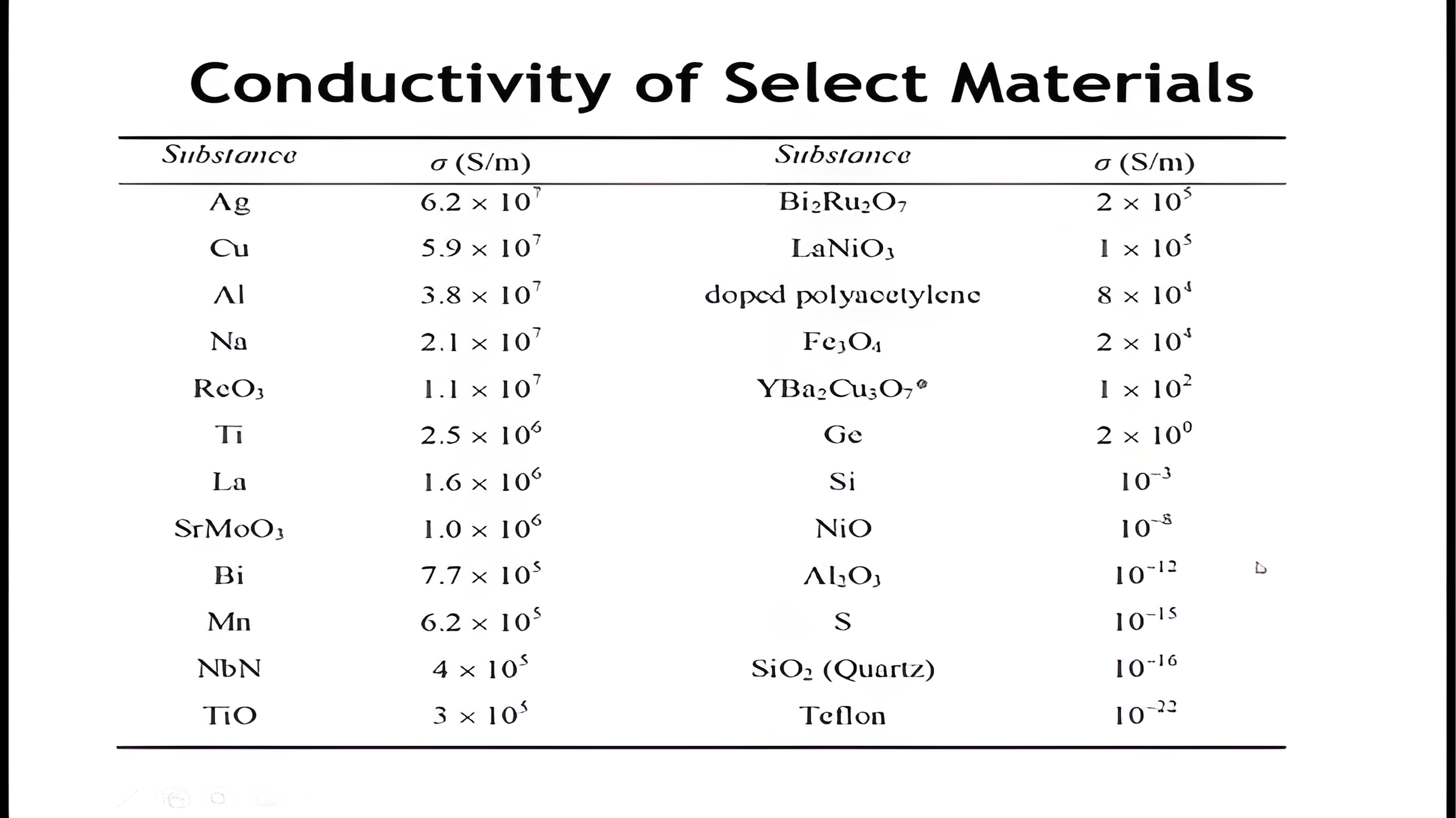
Conductivity of Select Materials
Organic Conductors: From Polymers to Nanotubes

Learning Objectives
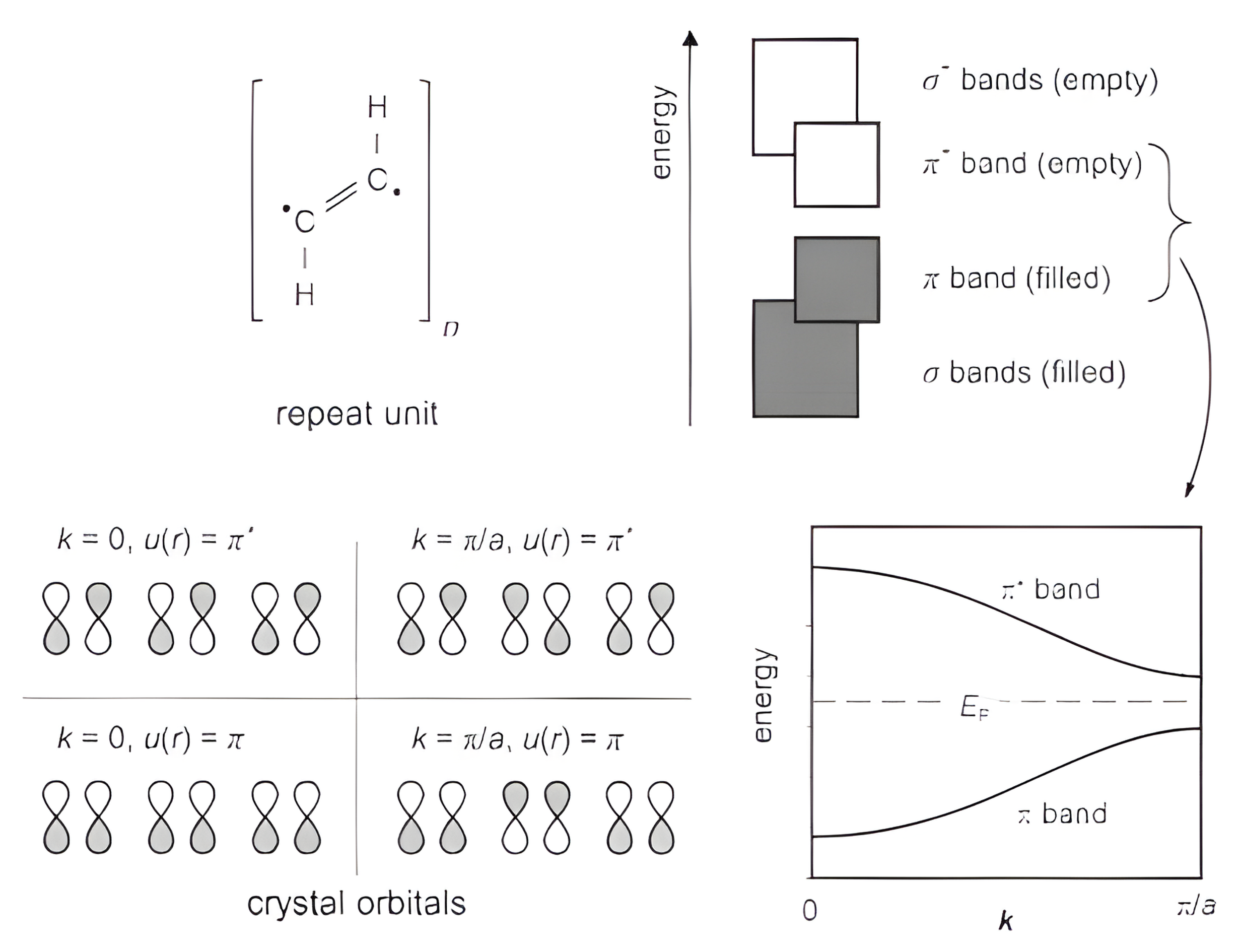
- Explain how π-conjugation leads to delocalized molecular orbitals that form bands
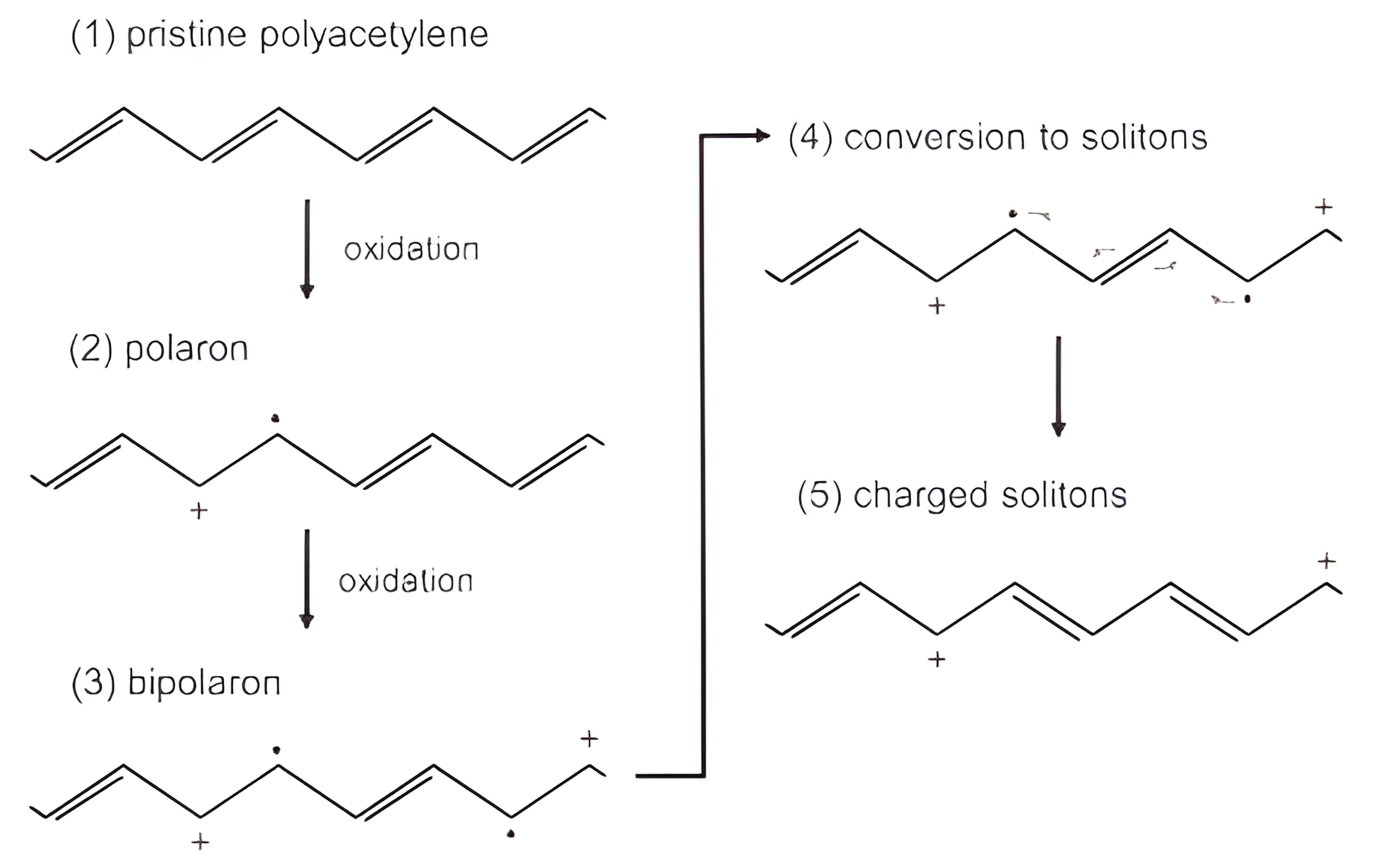
- Relate Peierls distortion and redox doping to the band gap and carrier formation in polymers
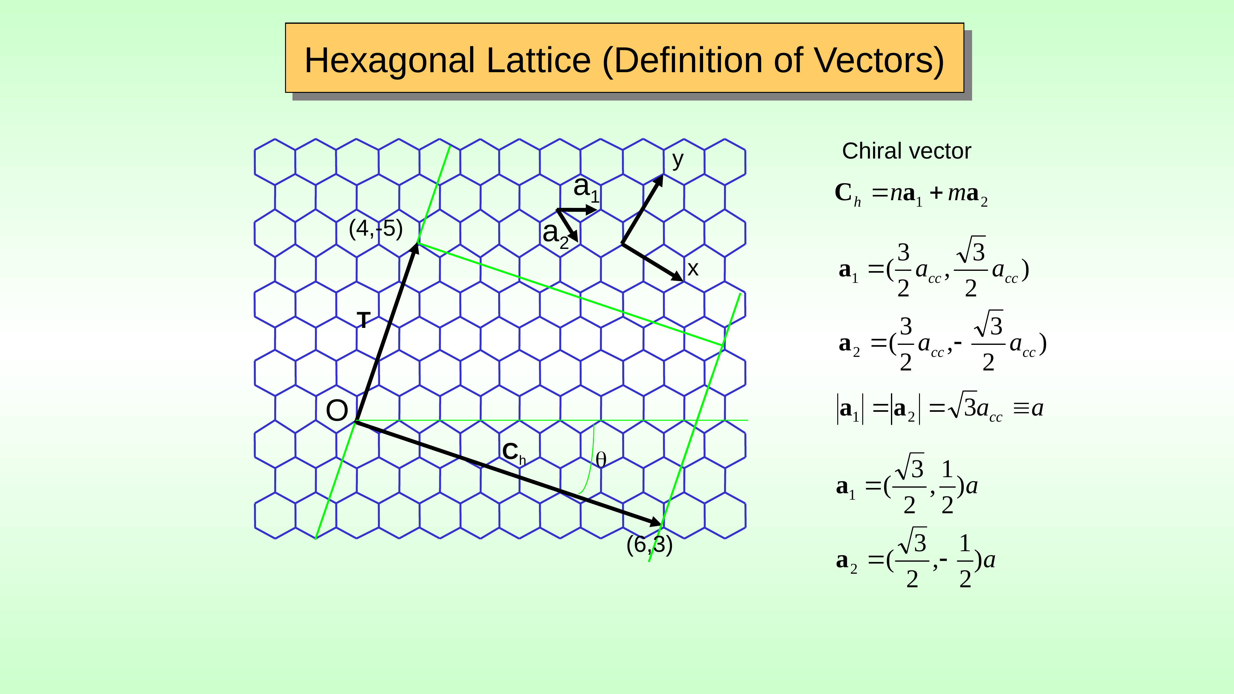
- Define nanotube (n,m) indices and compute diameter and chiral angle
- Predict metallic vs semiconducting behavior from the (n−m)/3 rule and Eg ∝ 1/d
- Compare transport limits in polymers vs nanotubes and link back to structure
Why Organic Conductors?
Breaking the Paradigm
- Traditional view: organics = insulators
- 1970s revolution: conjugated systems conduct
- Conductivity spans 15 orders of magnitude
- 2000 Nobel Prize in Chemistry
Key Advantages
- Lightweight & flexible
- Solution processable
- Tunable properties
- Applications: OLEDs, solar cells, sensors
Organic Electronics: Market Snapshot
| Application Area | Estimated Market Size (USD) | Notes |
|---|---|---|
| OLED / Organic Electronics (displays, flexible devices) | ~46B | By far the largest real-world use of organic conductors; includes OLED materials and organic layers in display stacks. |
| Conductive Polymers (coatings, EMI shielding, antistatic, electronics) | ~5B | Pure organic conductor materials used in coatings, components, printed electronics interfaces. |
| Organic Photovoltaics / Polymer Solar Cells | ~1.7B | Rapid growth; still small compared with displays but expanding quickly. |
| Sensors, Actuators, Printed Electronics | ~0.8B | Includes wearables, IoT devices, smart materials using organic conductors. |
| Bioelectronics / Medical & Wearable Interfaces | 0.1–1B (varies) | Highly specialized; smaller but high-value and growing. |
Teflon vs. trans-Polyacetylene
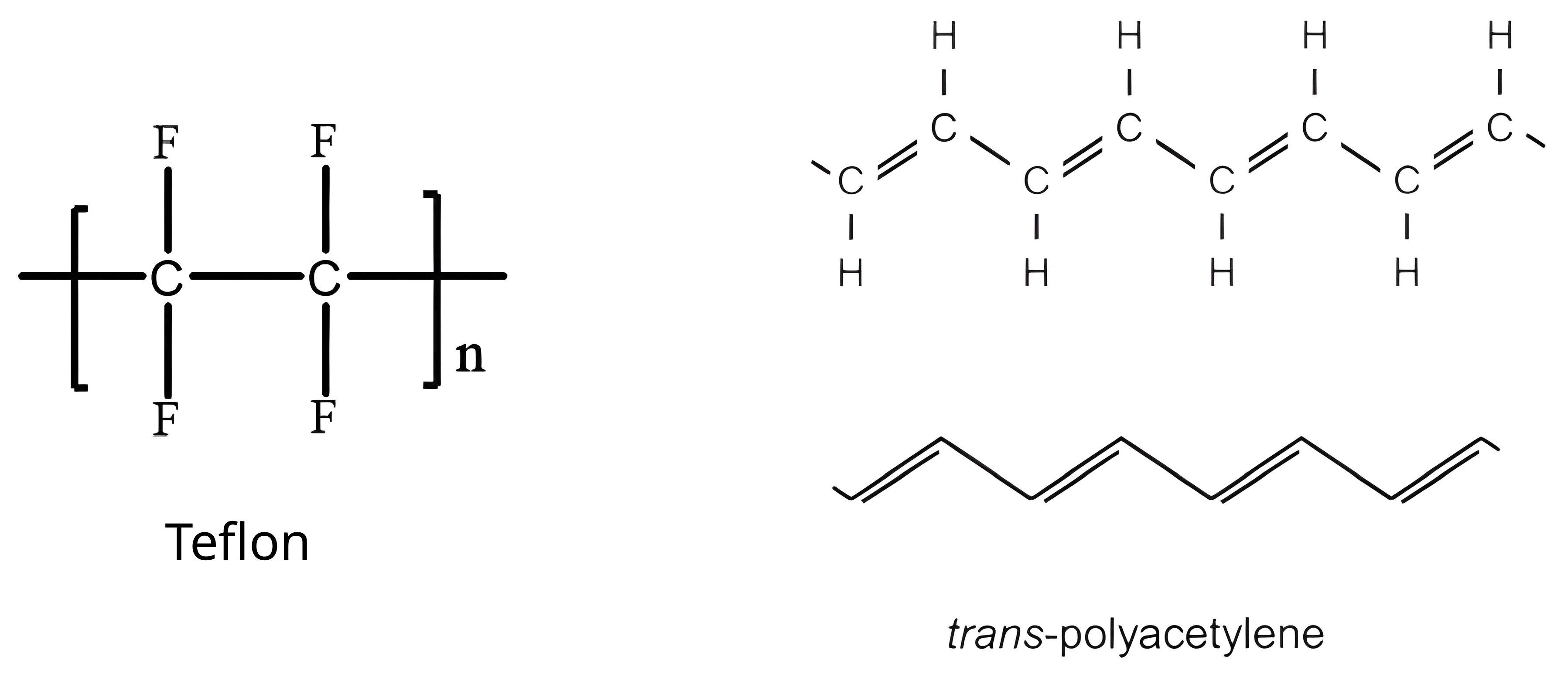
The $\pi$ and $\pi^*$ Bands of trans-Polyacetylene
Doping Polyacetylene: Polarons, Bipolarons, Solitons
PEDOT:PSS
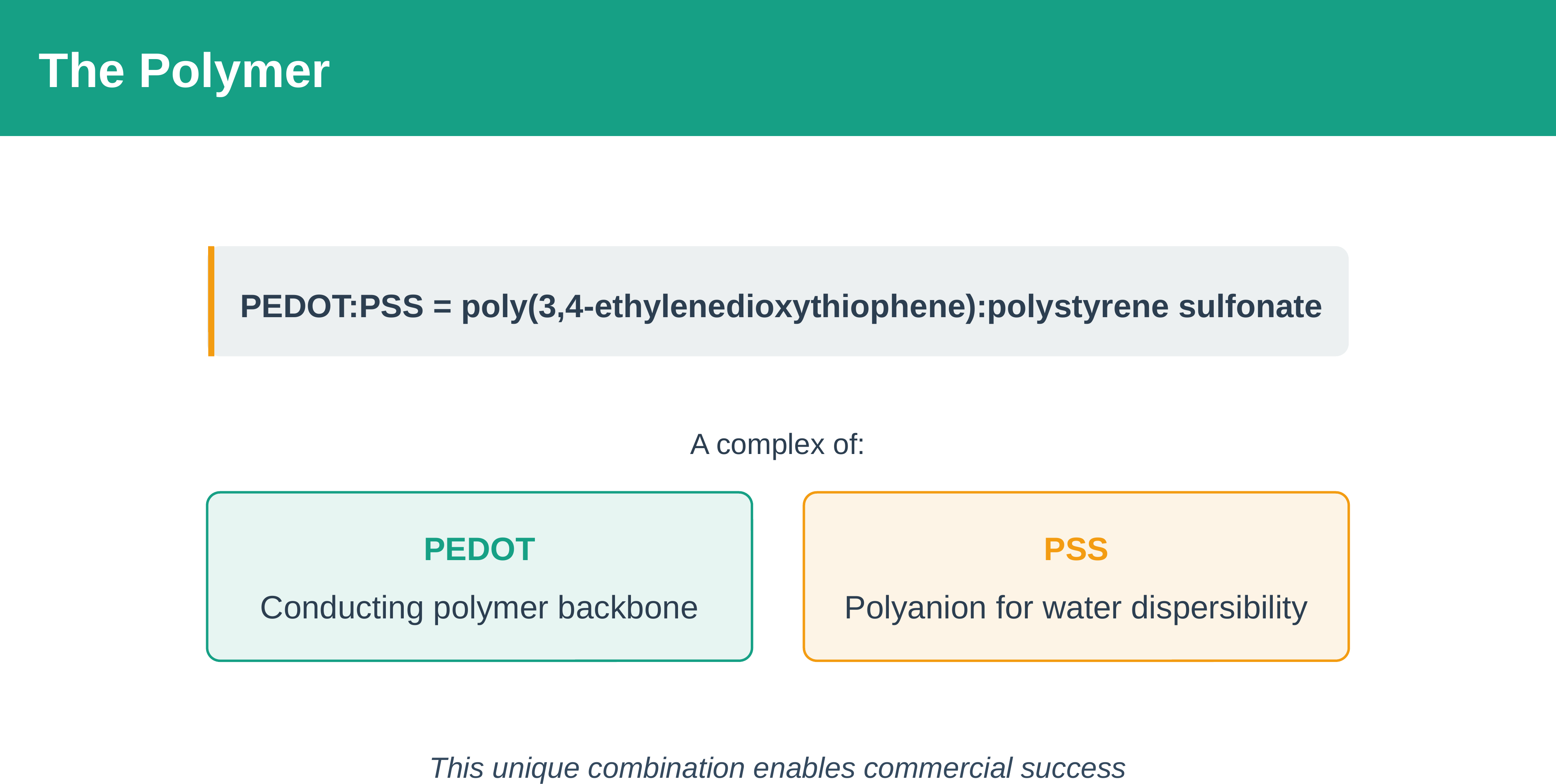
PEDOT and PSS Structures
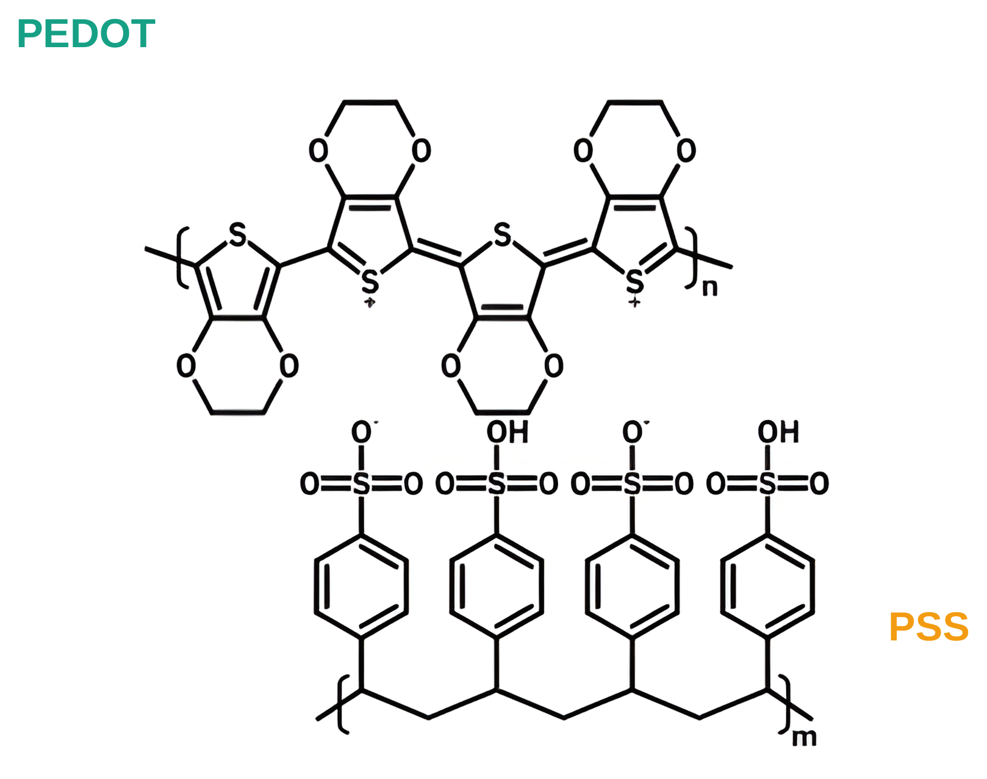
Key Advantage #1: Water Processable
The single biggest reason for commercial success
Processing Methods
- Solution casting at room temperature
- Spin coating
- Screen printing
- Roll-to-roll compatible
- Standard coating tools
Competitive Advantage
Other conducting polymers require:
- Harsh organic solvents
- In-situ oxidative polymerization
- Special handling conditions
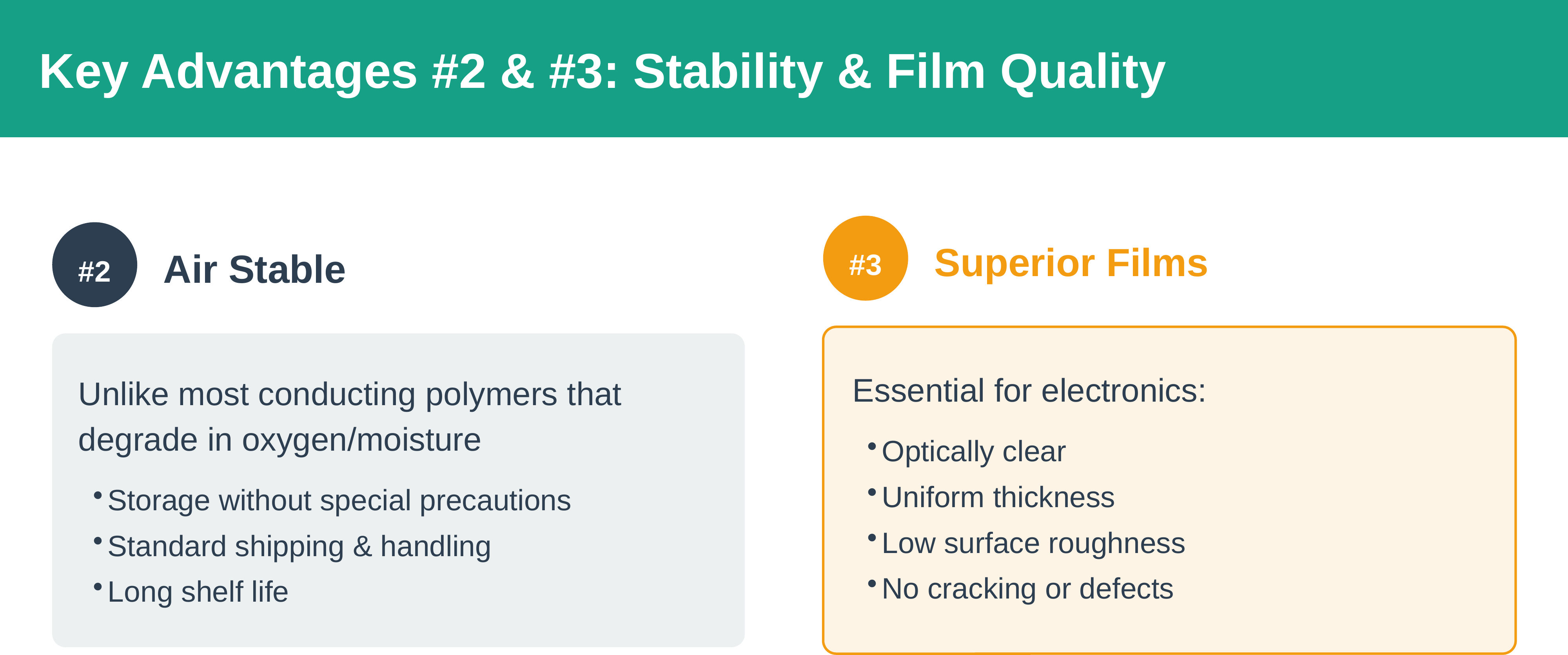
Key Advantages #2 & #3: Stability & Film Quality
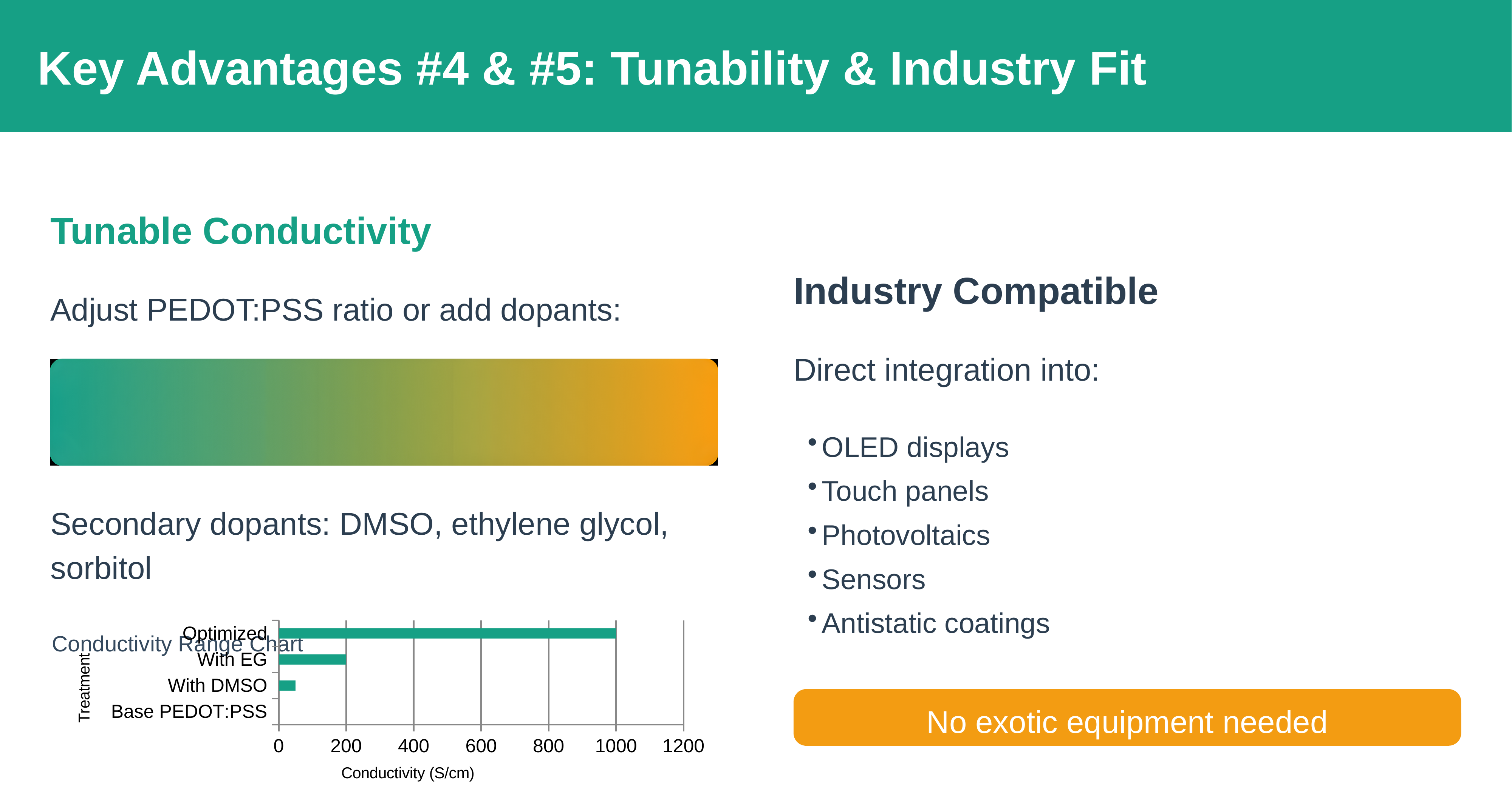
Key Advantages #4 & #5: Tunability & Industry Fit
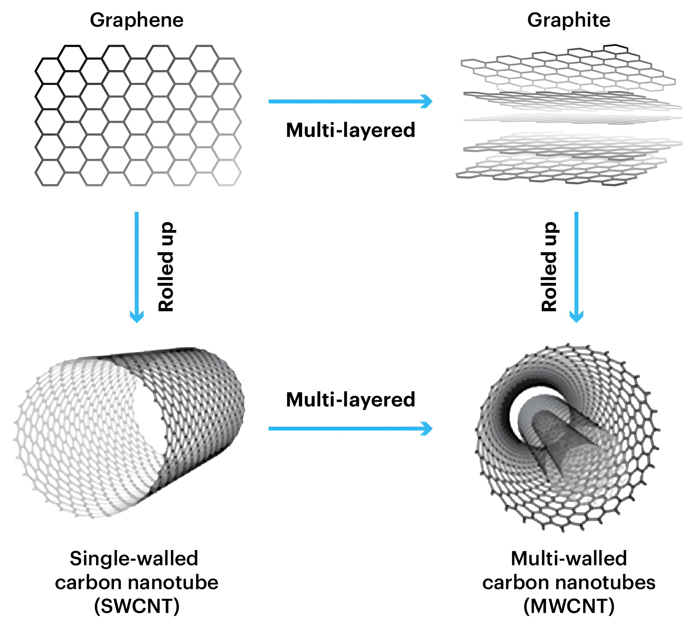
Single-Walled and Multi-Walled Carbon Nanotubes
Defining the Chiral Vector
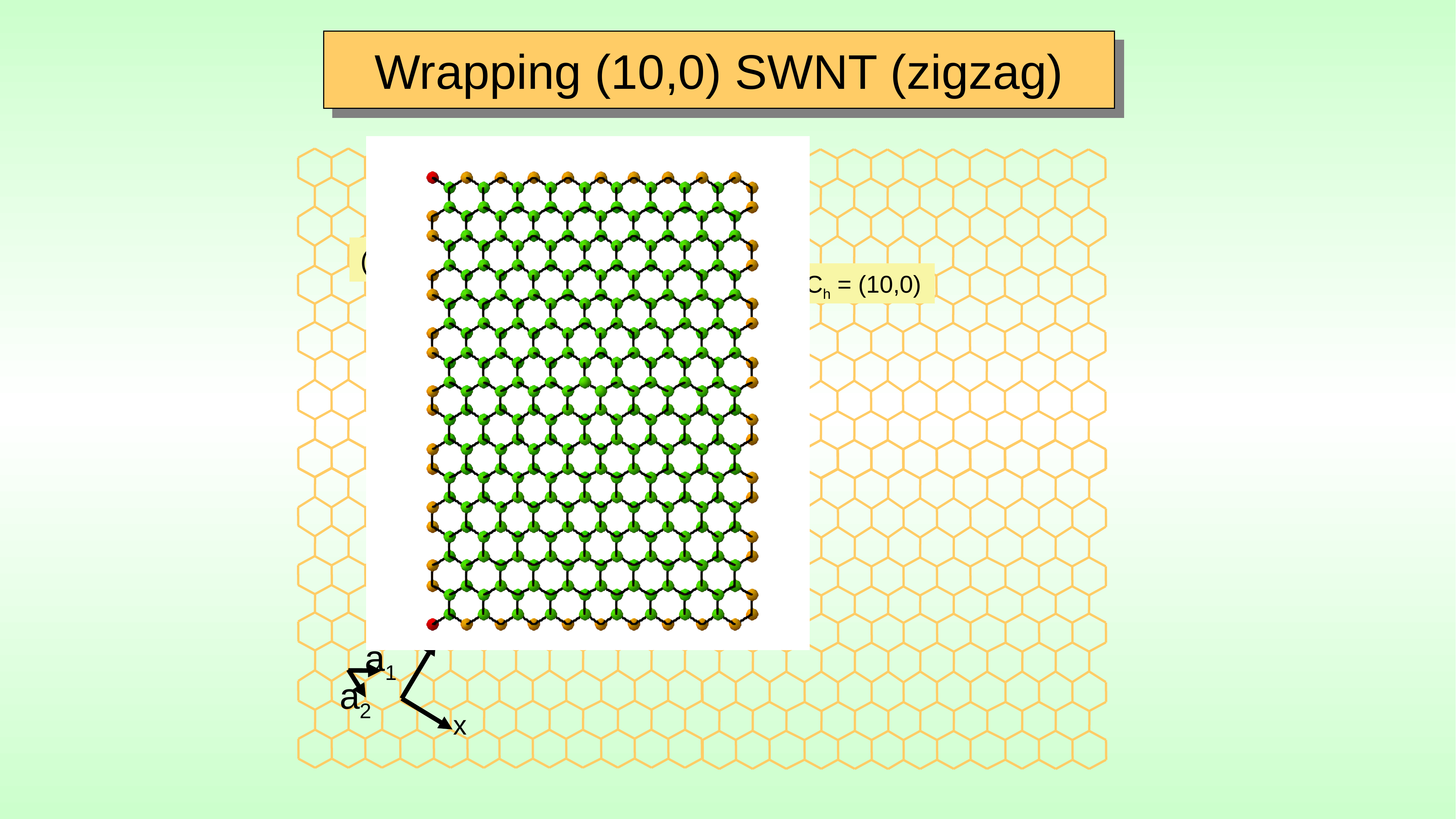
Wrapping the (10,0) Zigzag Nanotube
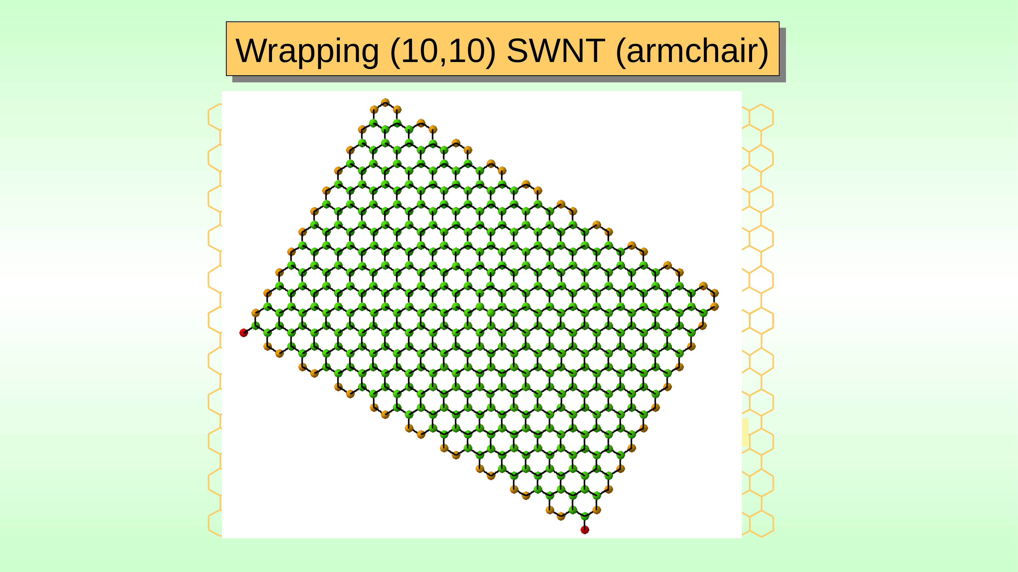
Wrapping the (10,10) Armchair Nanotube
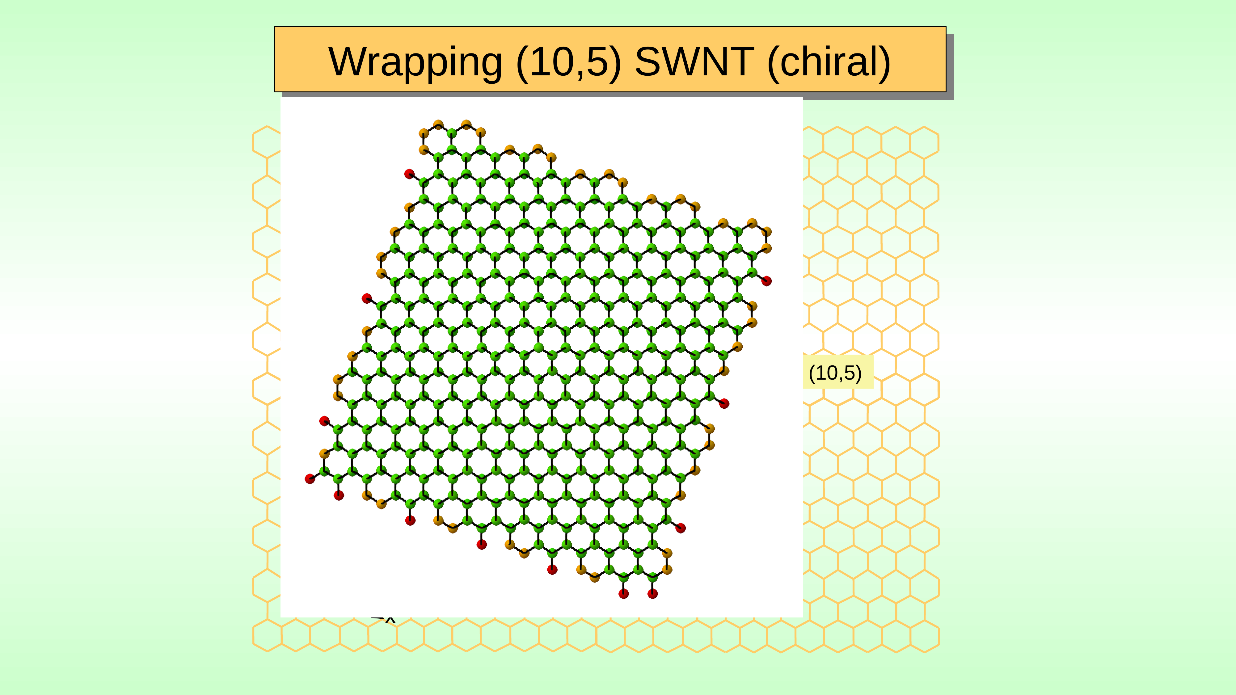
Wrapping the (10,5) Chiral Nanotube
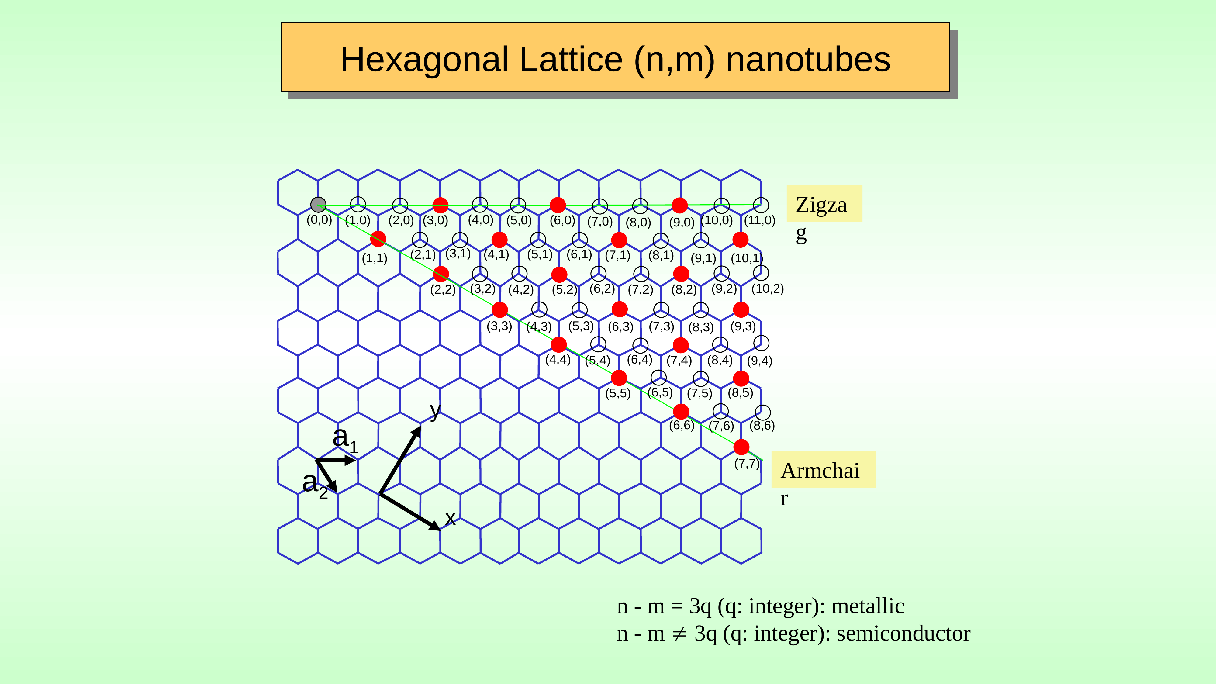
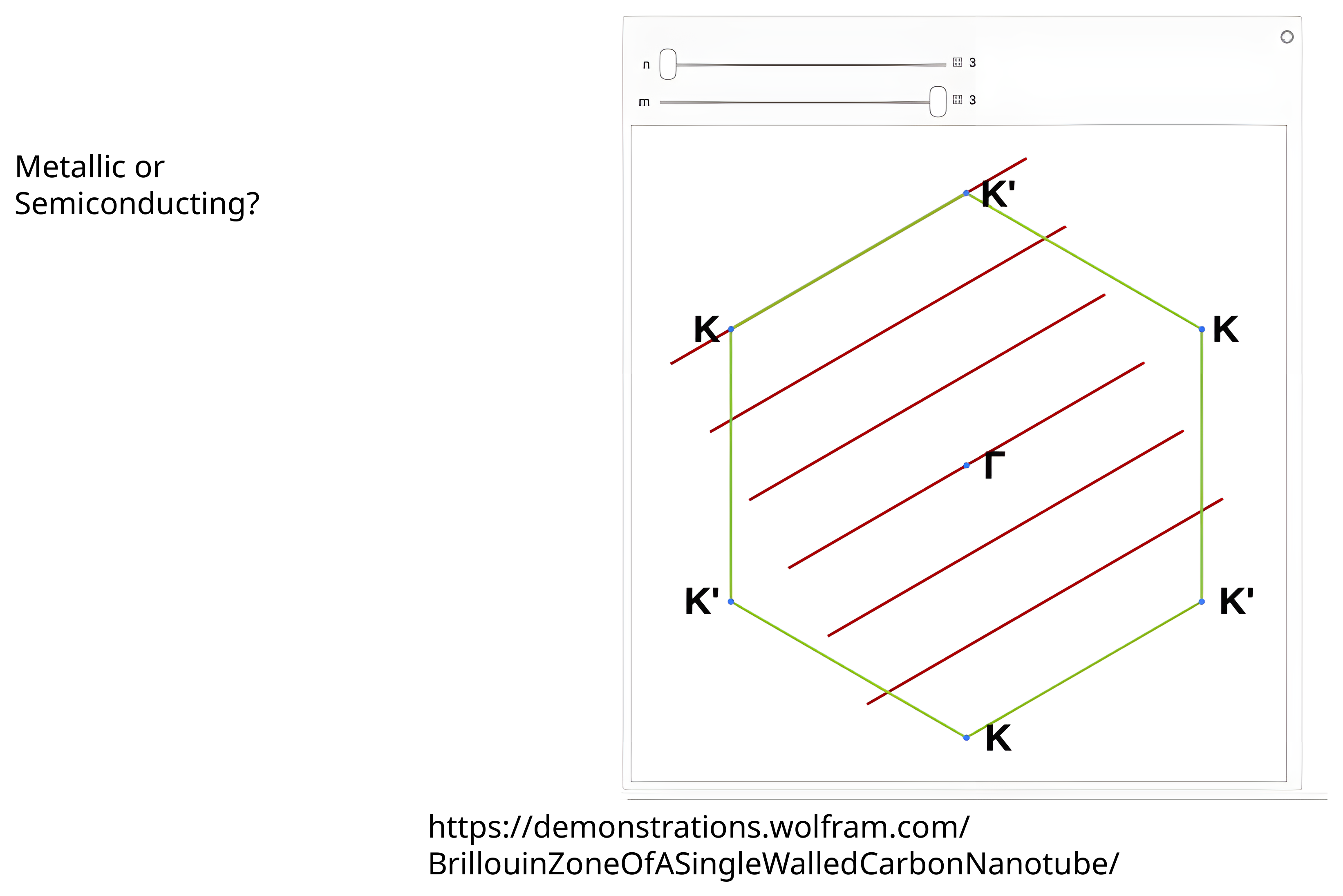
The (n,m) Map: Metallic or Semiconducting
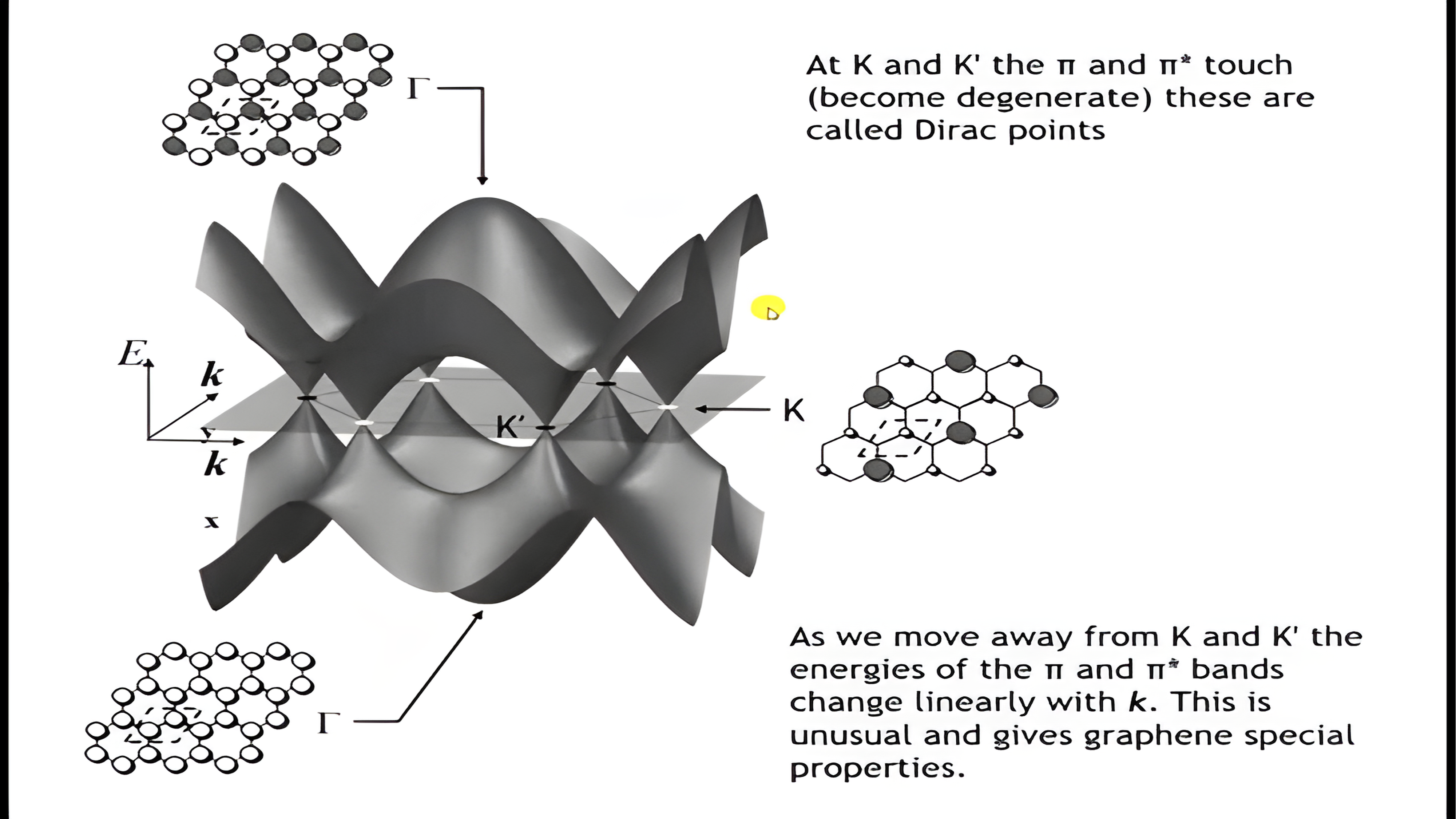
Graphene's Dirac Points
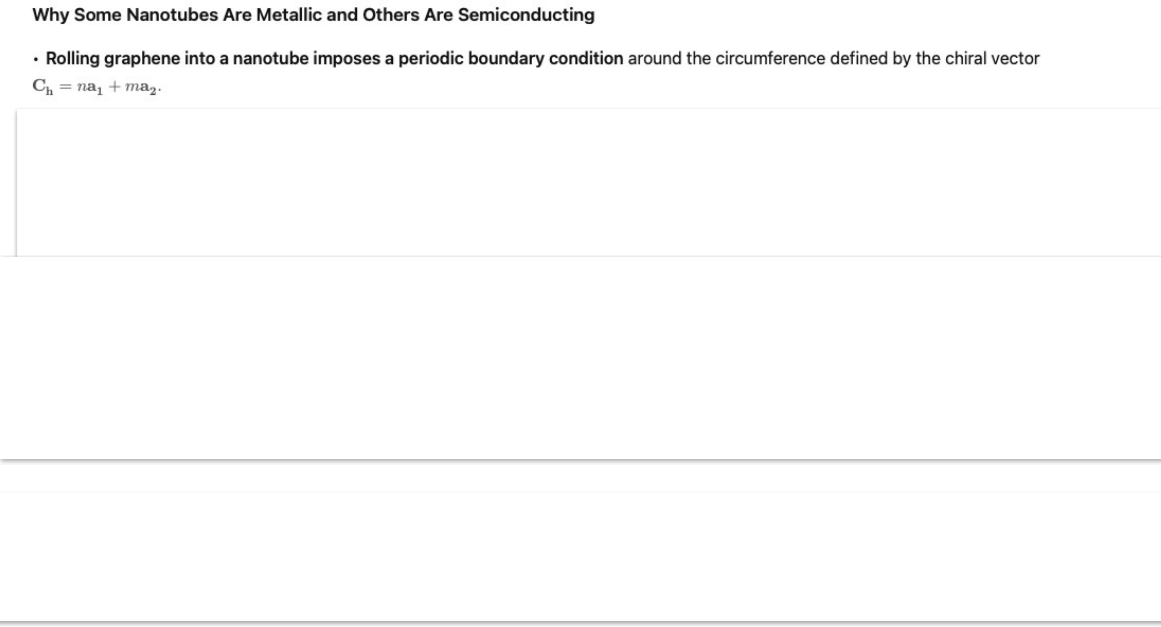
Why Some Nanotubes Are Metallic
Metallic or Semiconducting?
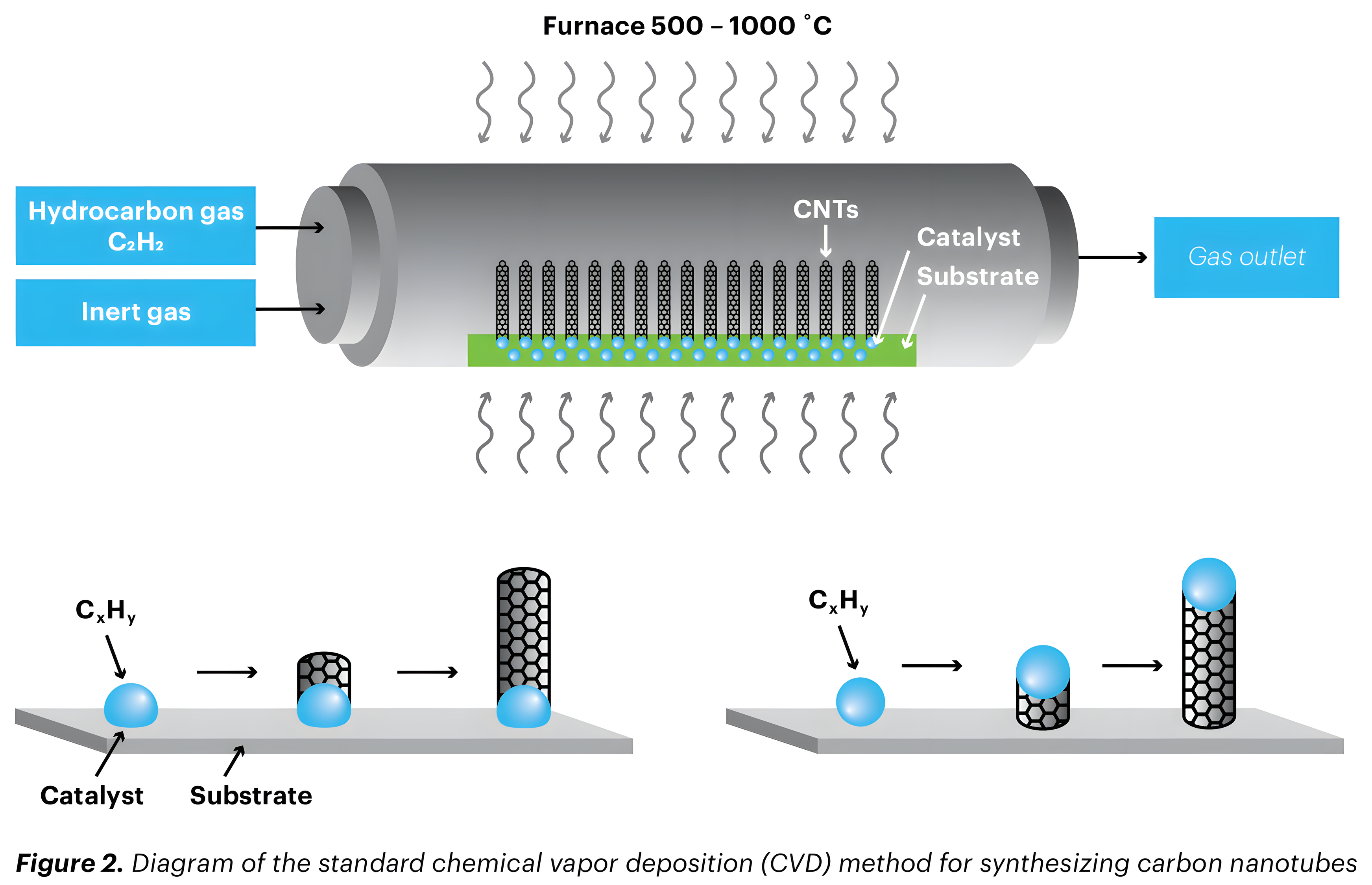
Carbon Nanotube Synthesis
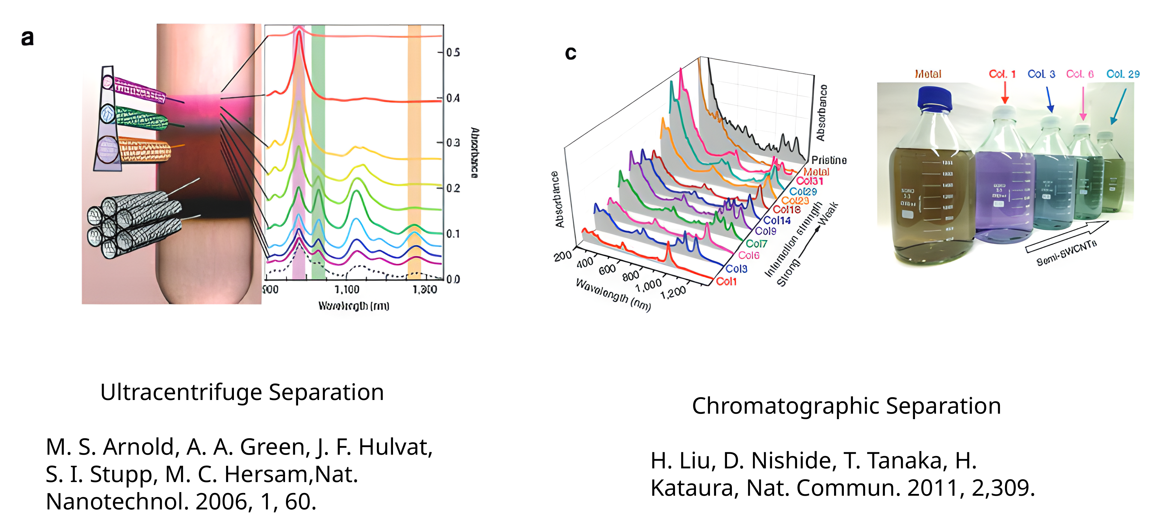
Separating Metallic from Semiconducting Tubes
Carbon Nanotube Markets
| Application Area | Estimated Market Size (USD) | Notes |
|---|---|---|
| CNT-enhanced composites (plastics, automotive, aerospace, sports equipment) | ~1.2–1.5B | Largest current CNT use; small CNT loadings improve conductivity, strength, ESD resistance; used in automotive fuel systems, EV lightweighting, structural materials. |
| CNT conductive additives for Li-ion batteries | ~0.9–1.1B | Fastest-growing segment; CNTs used as conductive networks in battery cathodes/anodes; driven by EV growth; increasingly replacing carbon black in high-performance cells. |
| Transparent / conductive films & coatings | ~0.2–0.3B | Used in flexible displays, touch panels, heaters; CNT films compete with ITO in specialty applications where flexibility or durability is required. |
| Sensors and electronics (RF devices, nanosensors, interconnects) | ~0.1–0.2B | Includes strain sensors, biosensors, gas sensors, and early nanoelectronic components; small market but high R&D intensity. |
| CNT powders, inks, dispersions | ~0.1B | Base materials sold as powders, masterbatches, dispersions; sold to electronics, composites, and energy manufacturers. |
Practice questions
Work the Lecture 21 practice questions before the next class. They cover π-conjugation and band formation in trans-polyacetylene, the Peierls distortion and the band gap it opens, redox doping with polarons, bipolarons and solitons, PEDOT:PSS and why it is water processable, the nanotube chiral vector and (n,m) indices, and the rule that decides whether a tube is metallic or semiconducting.
Open the Lecture 21 practice questions
Every question carries a worked explanation, so you can check your reasoning as you go.