CHEM 548: Materials Chemistry
Lecture 20: Semiconductors and the Conductivity of Transition Metal Compounds
Reading: Woodward, Karen, Evans, and Vogt, Solid State Materials Chemistry
Ch. 10 §§10.2–10.4
Learning Objectives: Semiconductors
By the end of this lecture, you will be able to:
- Explain the origin of low conductivity in intrinsic semiconductors and the role of band gaps in limiting charge carrier concentration
- Describe donor and acceptor doping mechanisms and their effects on semiconductor conductivity through band structure modifications
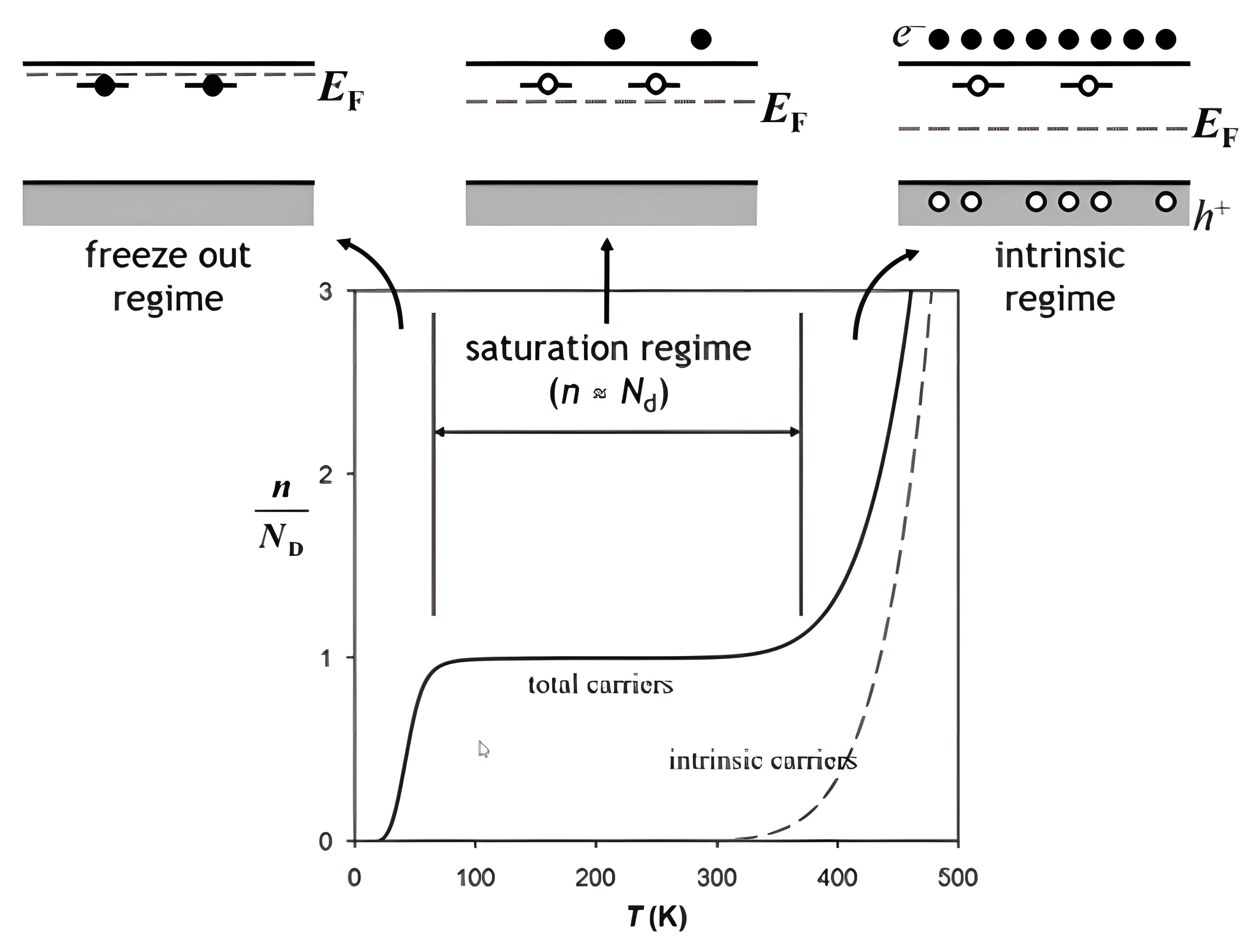
- Understand the temperature dependence of semiconductor conductivity including freeze-out, saturation, and intrinsic regimes
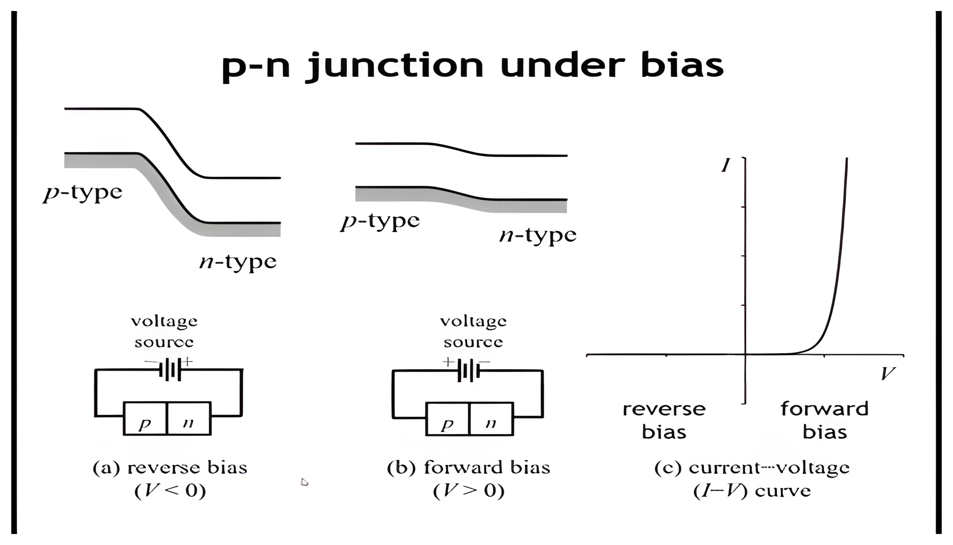
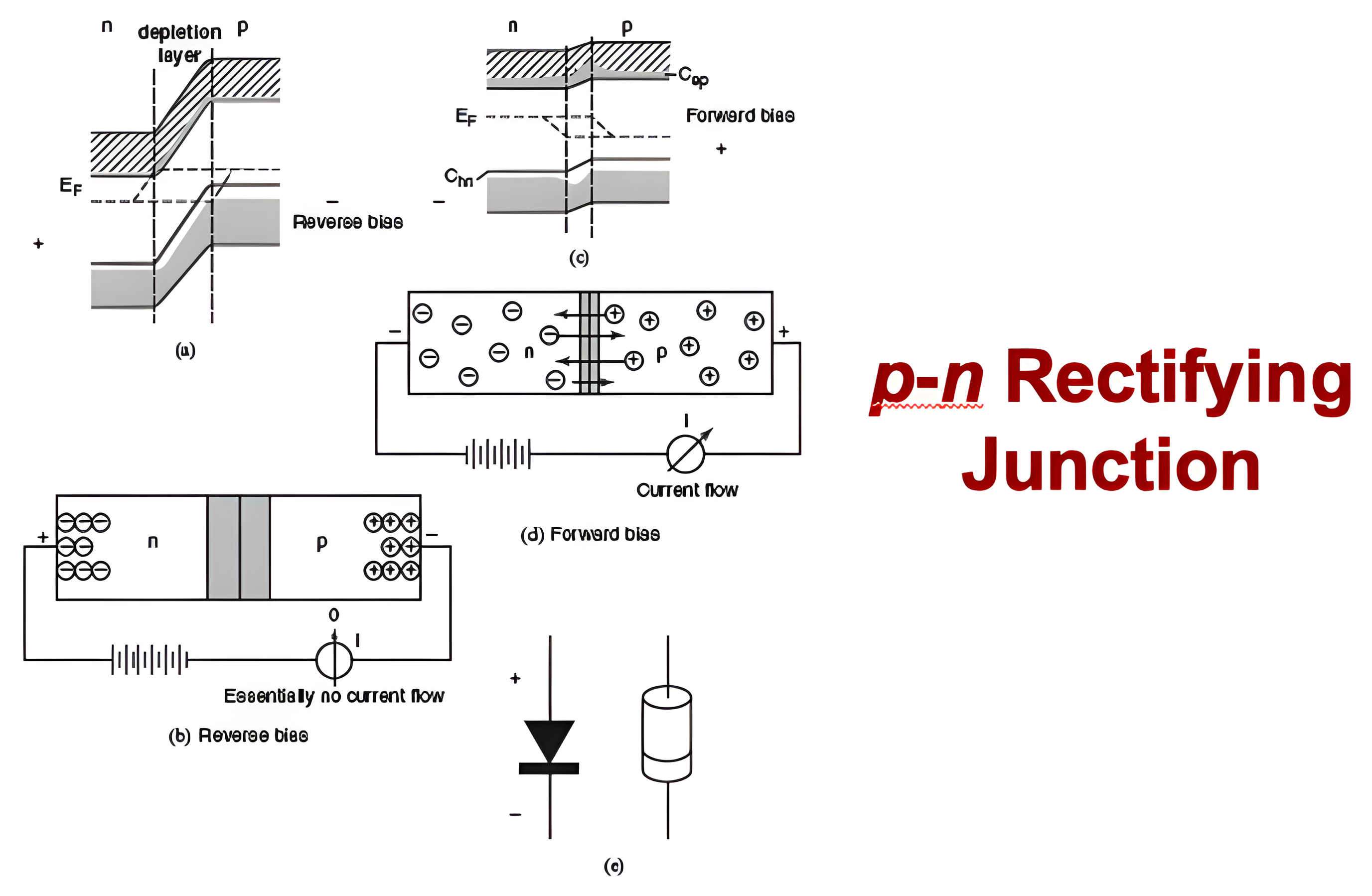
- Explain P-N junction behavior including rectification, band bending, and the formation of depletion regions
- Describe practical applications: photovoltaic cells, light-emitting diodes (LEDs), and metal-oxide-semiconductor field-effect transistors (MOSFETs)
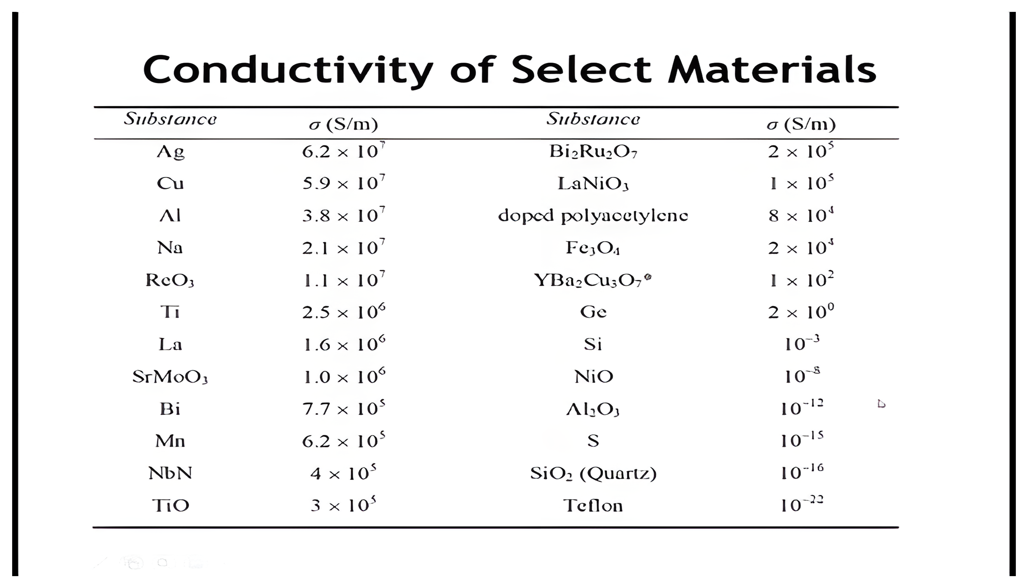
Conductivity of Select Materials
| Substance | σ (S/m) | Substance | σ (S/m) |
|---|---|---|---|
| Ag | 6.2 × 10⁷ | Bi₂Ru₂O₇ | 2 × 10⁵ |
| Cu | 5.9 × 10⁷ | LaNiO₃ | 1 × 10⁵ |
| Al | 3.8 × 10⁷ | doped polyacetylene | 8 × 10⁴ |
| Na | 2.1 × 10⁷ | Fe₃O₄ | 2 × 10⁴ |
| ReO₃ | 1.1 × 10⁷ | YBa₂Cu₃O₇ | 1 × 10² |
| Ti | 2.5 × 10⁶ | Ge | 2 × 10⁰ |
| La | 1.6 × 10⁶ | Si | 10⁻³ |
| SrMoO₃ | 1.0 × 10⁶ | NiO | 10⁻⁸ |
| Bi | 7.7 × 10⁵ | Al₂O₃ | 10⁻¹² |
| Mn | 6.2 × 10⁵ | S | 10⁻¹⁵ |
| NbN | 4 × 10⁵ | SiO₂ (Quartz) | 10⁻¹⁶ |
| TiO | 3 × 10⁵ | Teflon | 10⁻²² |
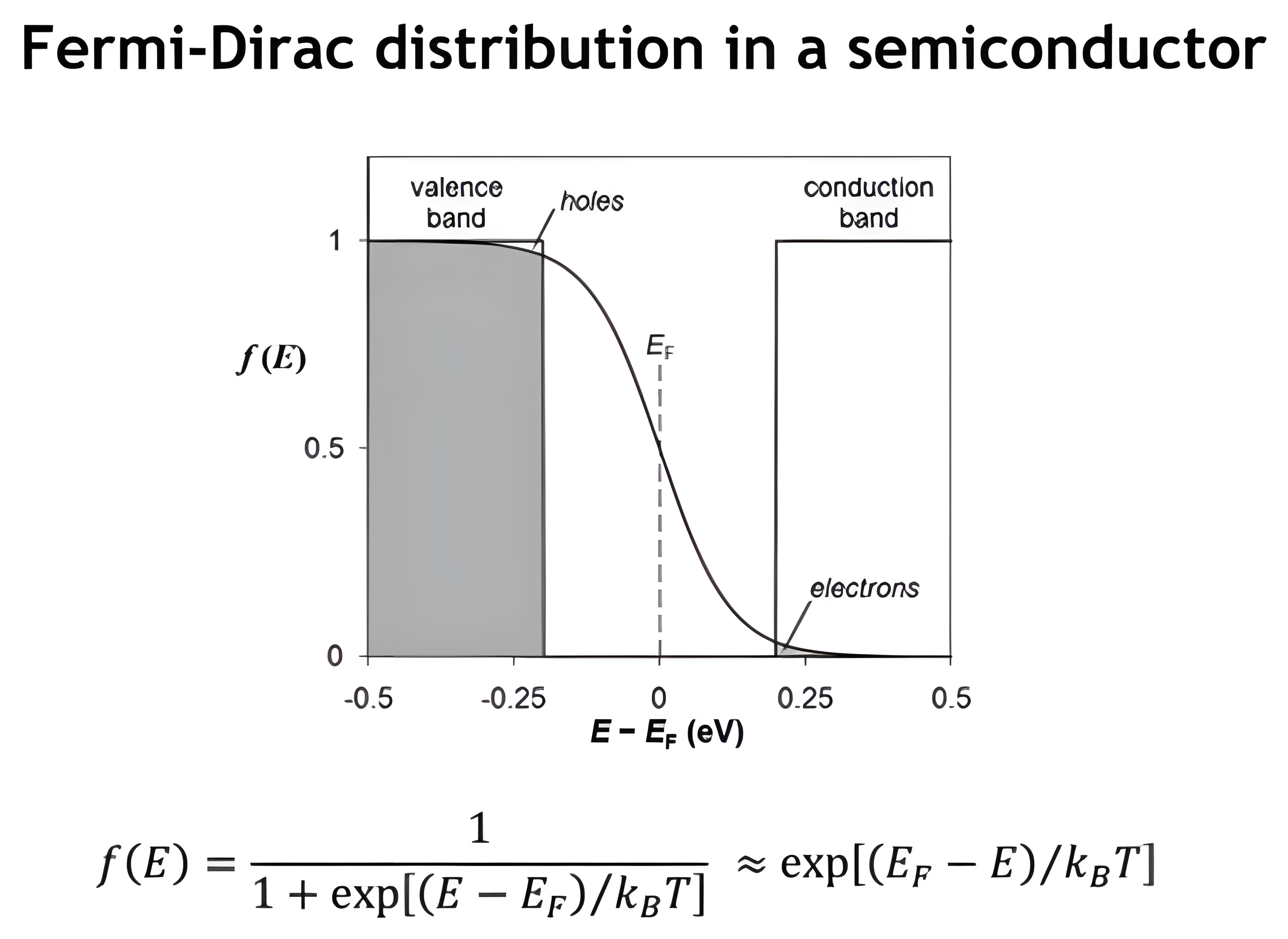
Fermi-Dirac Distribution in a Semiconductor
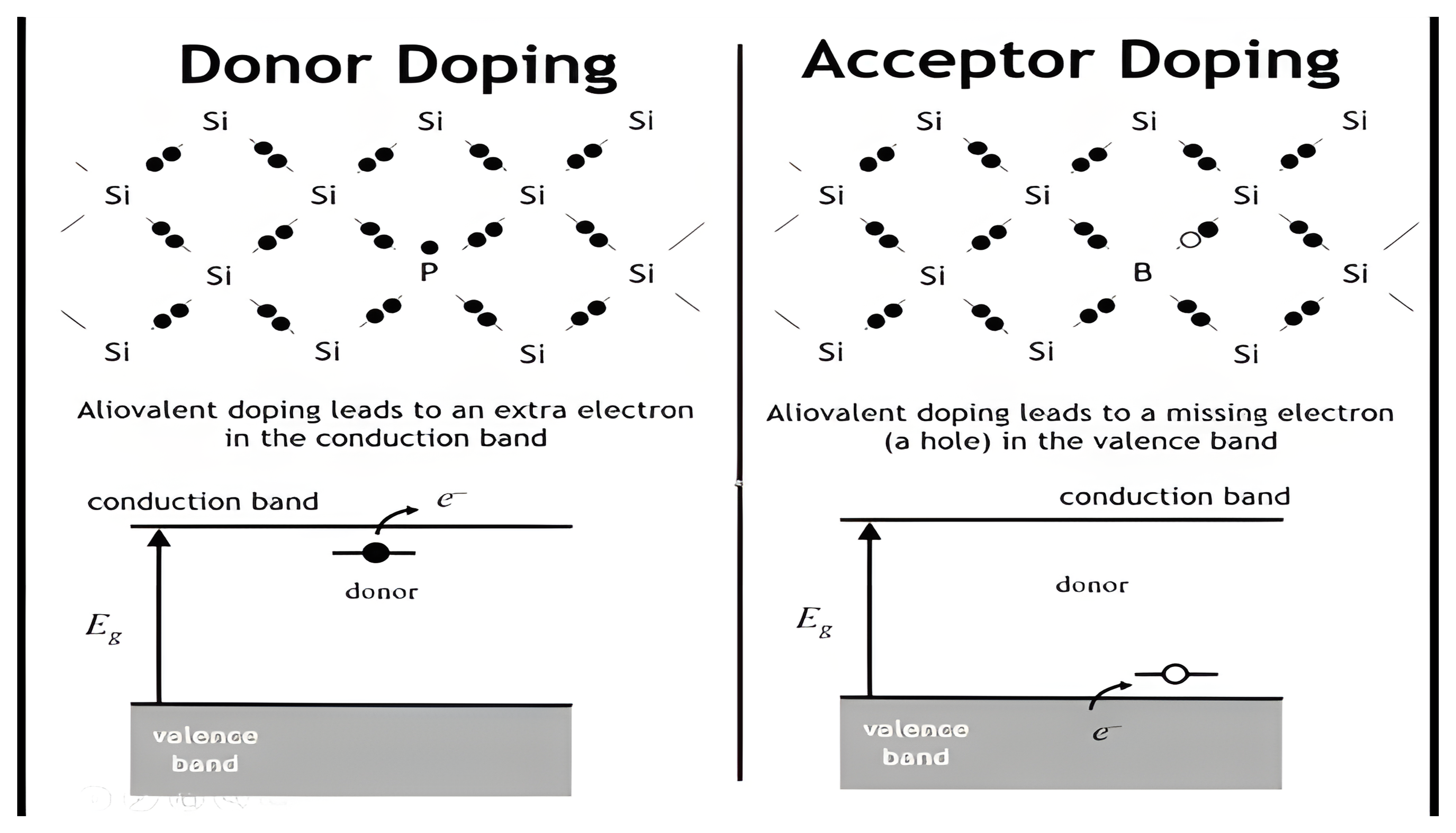
Donor and Acceptor Doping
Hydrogenic type orbital in a donor doped semiconductor
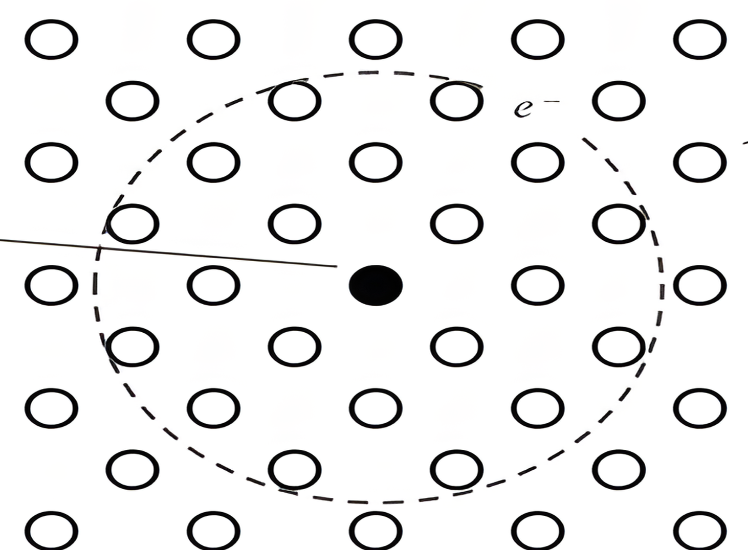
Black dot: positively charged dopant (e.g. PSi•). Open circles: host lattice atom (e.g. Si). Dashed circle: the donated e⁻.
rd = εr (me/m*) 0.053 nm
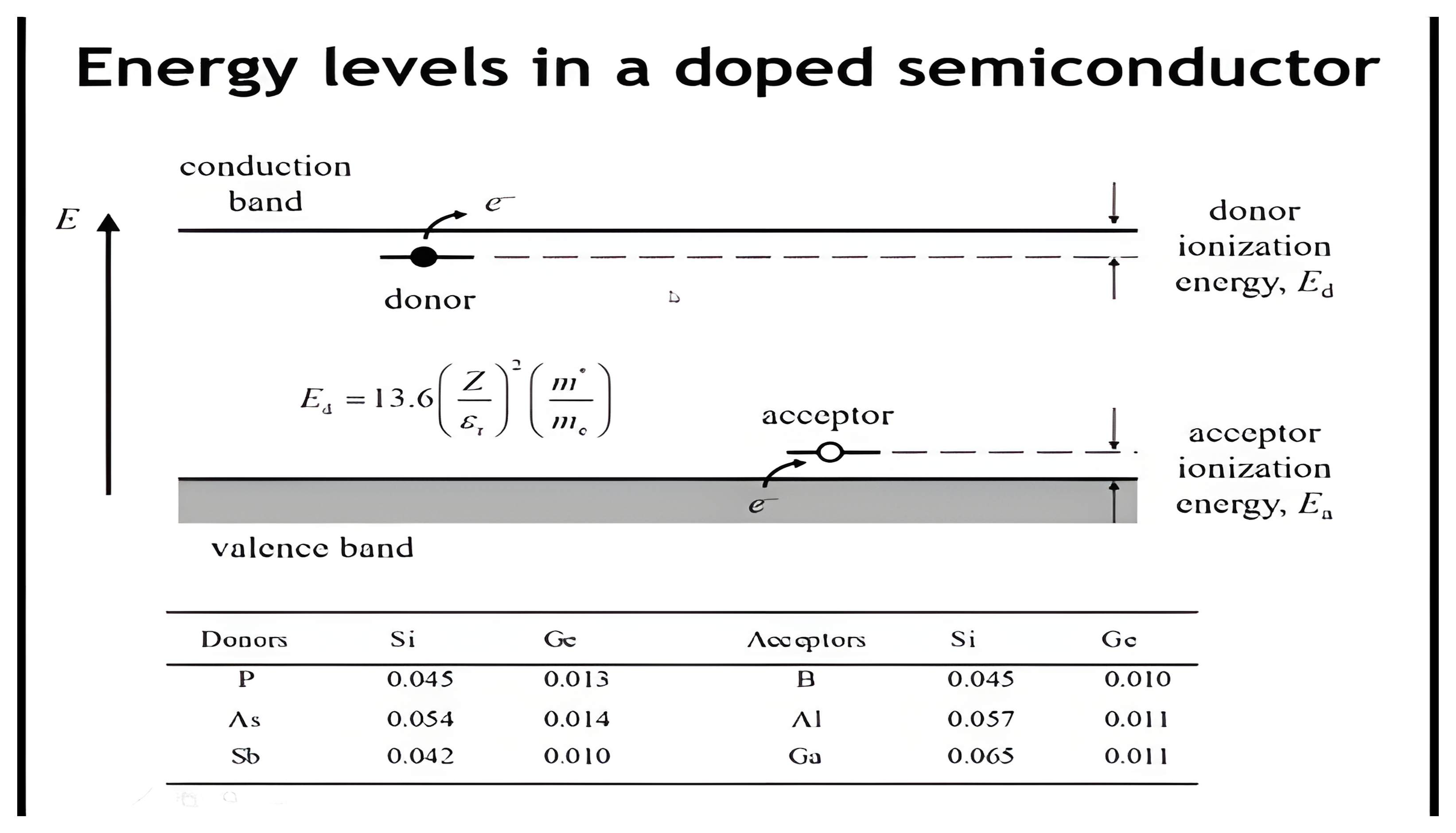
Energy Levels in a Doped Semiconductor
Carrier Concentration vs. Temperature
Mobility and Conductivity
| Eg (eV) | μe (m²V⁻¹s⁻¹) | μh (m²V⁻¹s⁻¹) | |
|---|---|---|---|
| Elements | |||
| Si | 1.11 (indirect) | 0.19 | 0.050 |
| Ge | 0.67 (indirect) | 0.38 | 0.182 |
| III–V | |||
| GaAs | 1.43 (direct) | 0.90 | 0.050 |
| InAs | 0.36 (direct) | 3.30 | 0.046 |
| InSb | 0.18 (direct) | 8.00 | 0.075 |
| II–VI | |||
| ZnS | 3.6 (direct) | 0.012 | 0.0005 |
| ZnSe | 2.58 (direct) | 0.053 | 0.0016 |
| CdTe | 1.50 (direct) | 0.030 | 0.0065 |
σ = σn + σp = nμee + pμhe
See Gradescope Quiz 1
1. What is the primary reason for the low conductivity of an intrinsic (pure) semiconductor like silicon?
2. When an acceptor dopant like boron (which has one fewer valence electron than silicon) is added, what type of charge carrier is created?
3. How does the conductivity of a semiconductor generally change as temperature increases (in the intrinsic regime)?
4.In a doped semiconductor, what is the "saturation regime"?
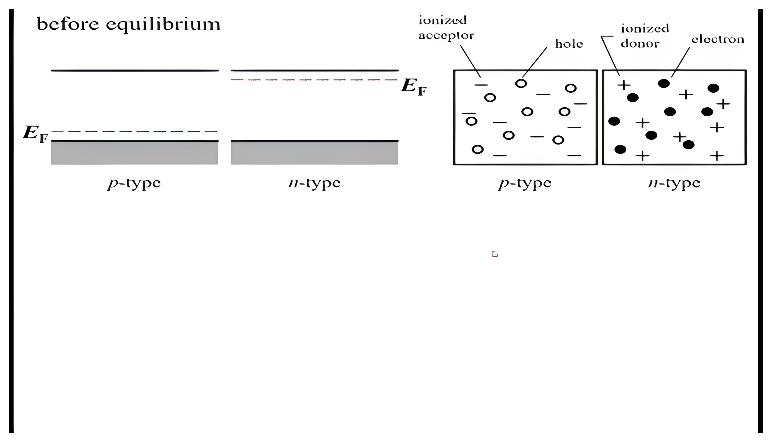
The p-n Junction
p-n Junction Under Bias
The p-n Rectifying Junction
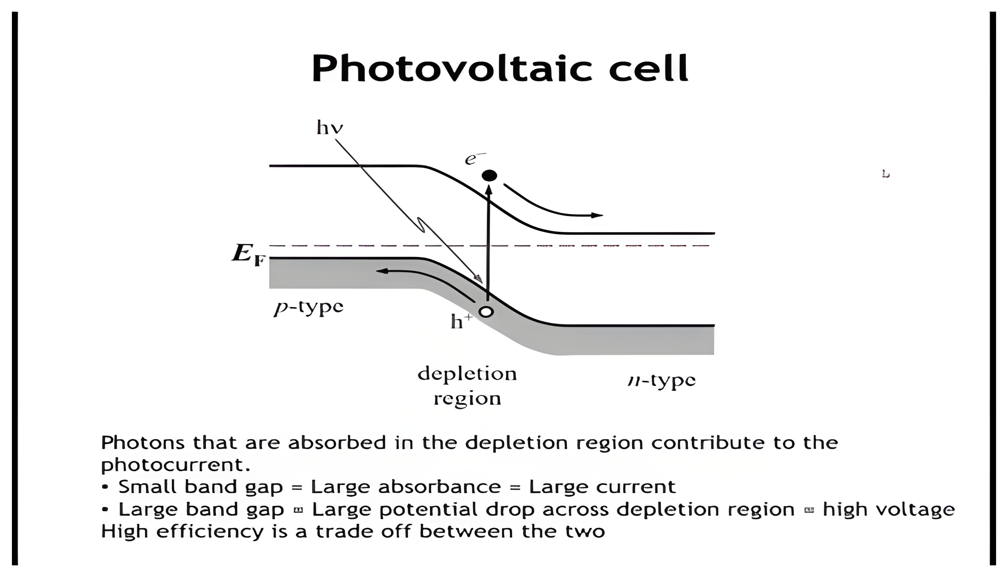
Photovoltaic Cell
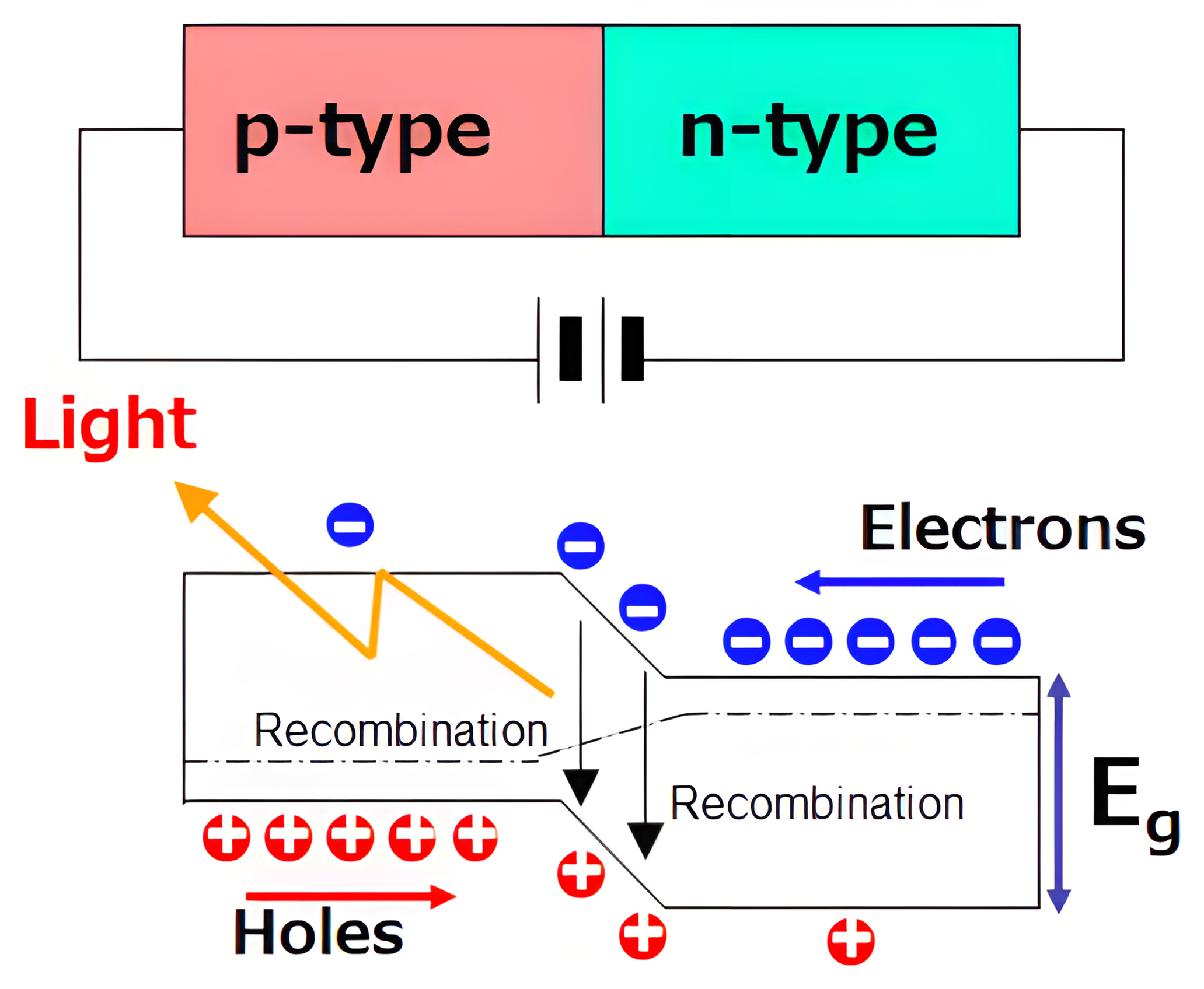
Light-Emitting Diode
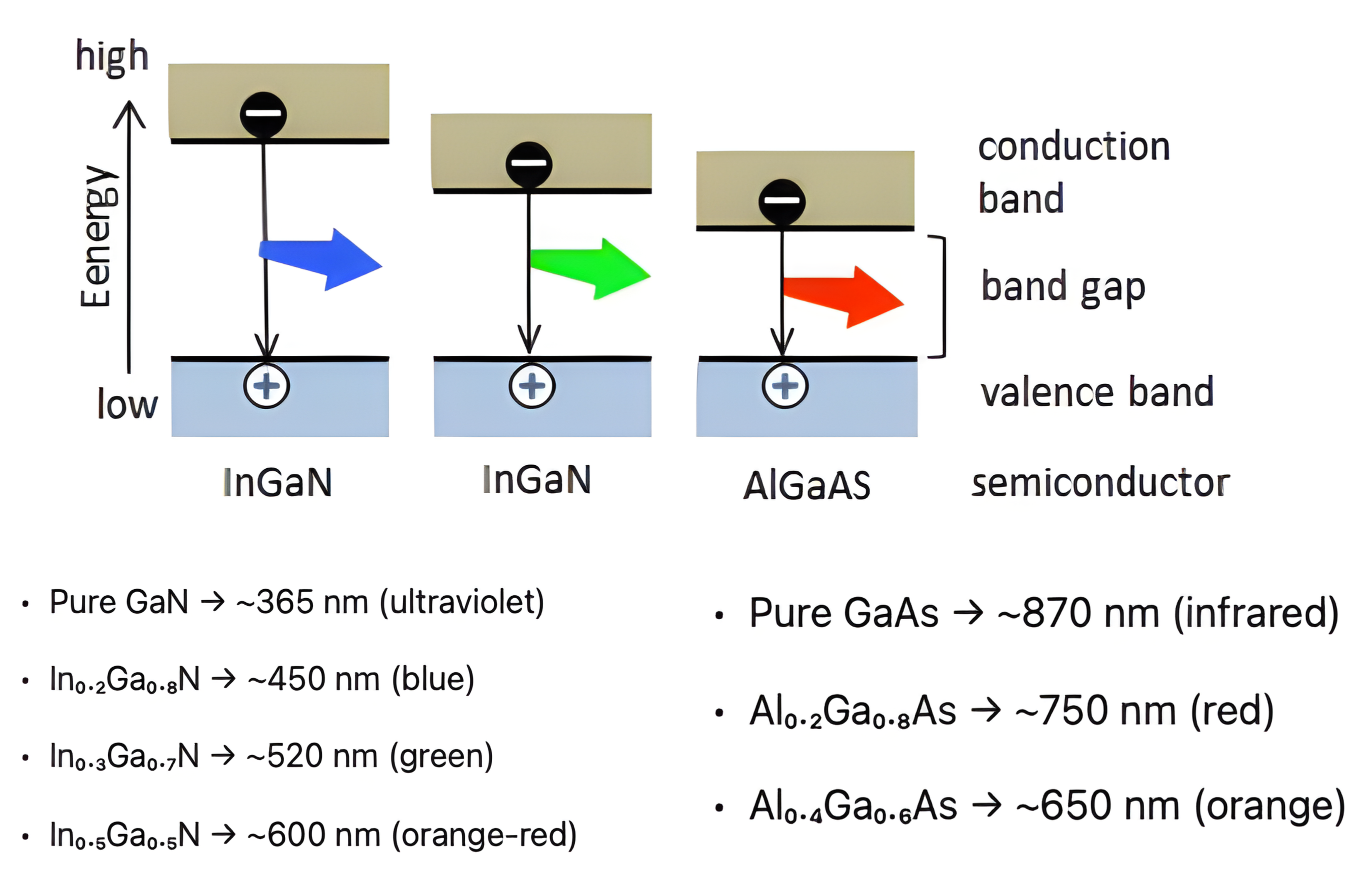
LED Colors and the Band Gap
Metal oxide field effect transistor (MOSFET)
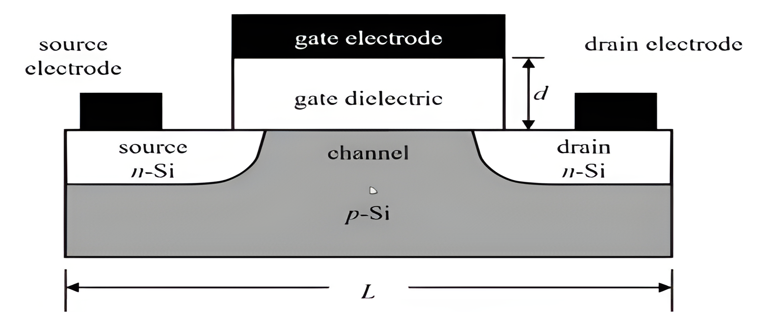
Cross-section labels: source electrode, gate electrode, gate dielectric of thickness d, drain electrode, source n-Si, channel, drain n-Si, p-Si substrate, channel length L.
| 2006 MOSFET | 2010 MOSFET |
|---|---|
| L = 65 nm | L = 32 nm |
| d = 1.2 nm | d = ~7 nm |
| Gate dielectric: SiO₂ (εr = 3.9) | Gate dielectric: HfO₂ (εr = 30) |
| Gate electrode: n-doped Si | Gate electrode: TiN |
Switching a MOSFET
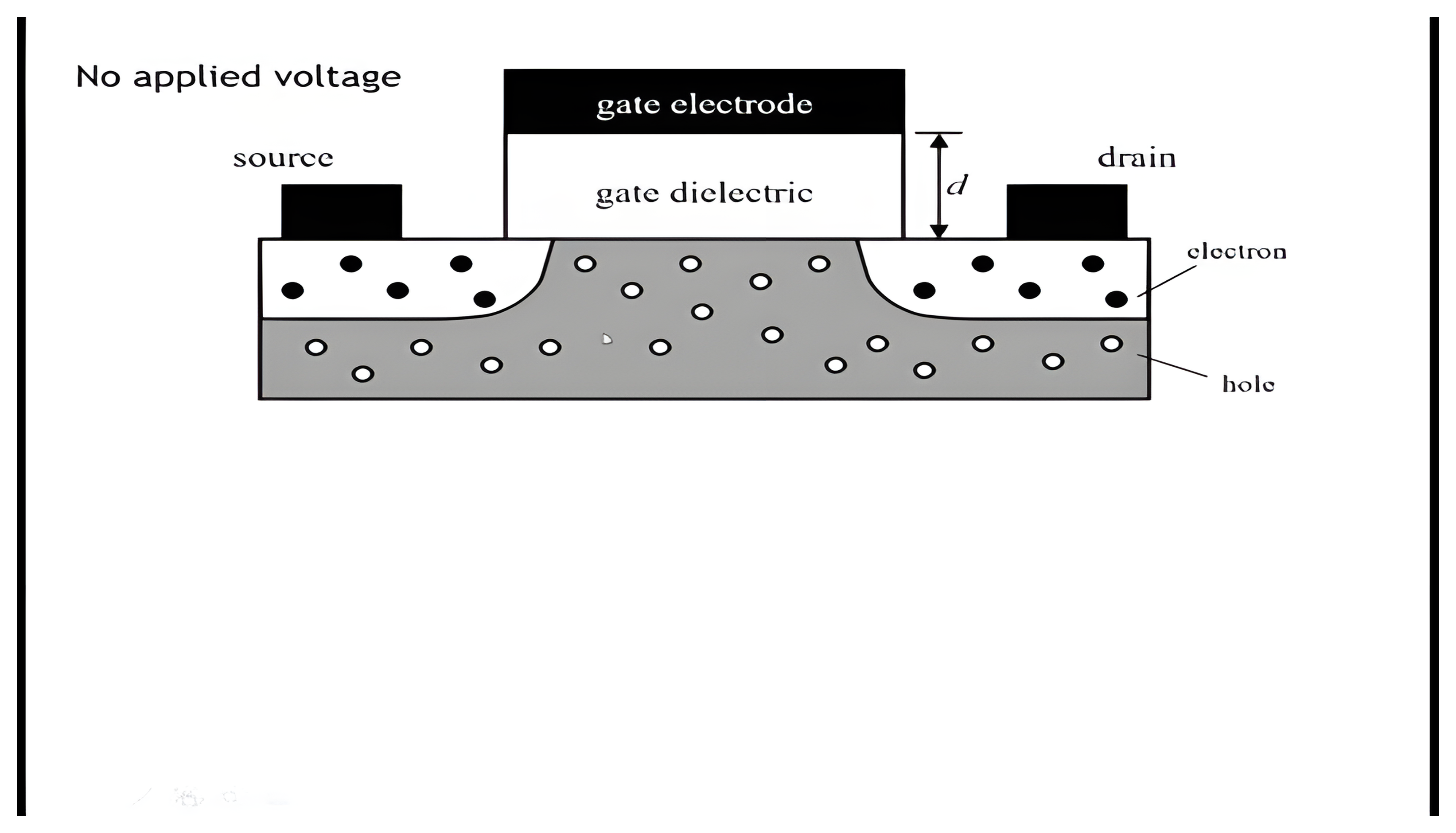
MOSFET Scaling and High-k Dielectrics
Metal oxide field effect transistor (MOSFET)
Cross-section labels: source electrode, gate electrode, gate dielectric of thickness d, drain electrode, source n-Si, channel, drain n-Si, p-Si substrate, channel length L.
| 2006 MOSFET | 2010 MOSFET |
|---|---|
| L = 65 nm | L = 32 nm |
| d = 1.2 nm | d = ~7 nm |
| Gate dielectric: SiO₂ (εr = 3.9) | Gate dielectric: HfO₂ (εr = 30) |
| Gate electrode: n-doped Si | Gate electrode: TiN |
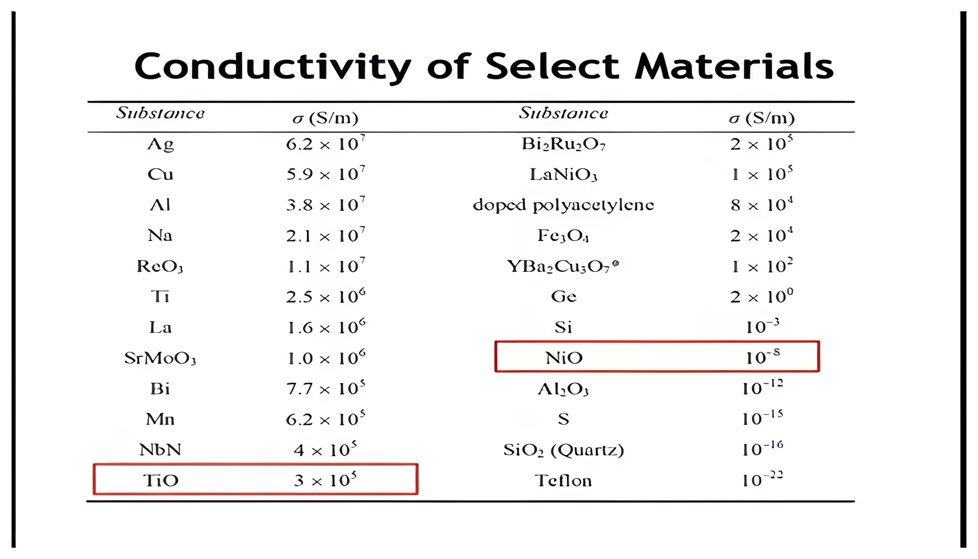
Conductivity of Select Materials: NiO and TiO
See Gradescope Quiz 2
1. In a p-n junction at equilibrium (no external voltage), what is the fundamental origin of the built-in electric field within the depletion region?
2. When a p-n junction is formed, the conduction and valence bands "bend" across the depletion region. What is the primary physical reason for this band bending?
3. Applying a reverse bias to a p-n junction (e.g., positive voltage to the n-type side) stops significant current flow. How does it accomplish this?
4. In an n-channel MOSFET built on a p-type substrate, how does applying a strong positive voltage to the gate electrode "turn on" the transistor?
5. Why was it necessary for the semiconductor industry to switch from silicon dioxide (SiO₂) to a high-k dielectric like hafnium oxide (HfO₂) for the gate?
Learning Objectives: Conductivity of Transition Metal Compounds
After this lecture, you will be able to:
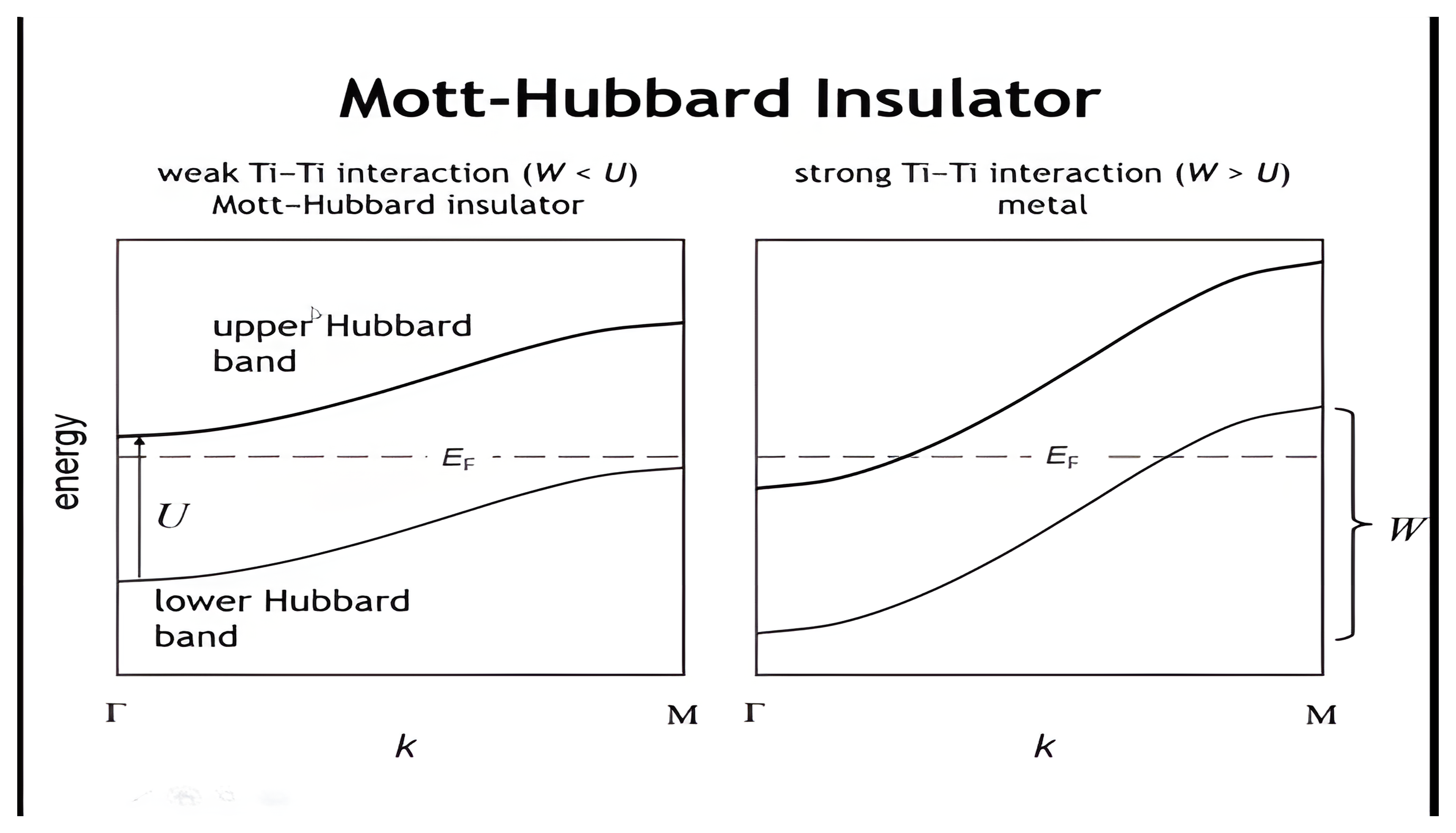
- Explain how electron-electron repulsions determine conductivity in transition metal compounds
- Apply the Hubbard model to predict metallic vs. insulating behavior by comparing bandwidth (W) and on-site repulsion (U)
- Identify Mott-Hubbard insulators and explain their origin
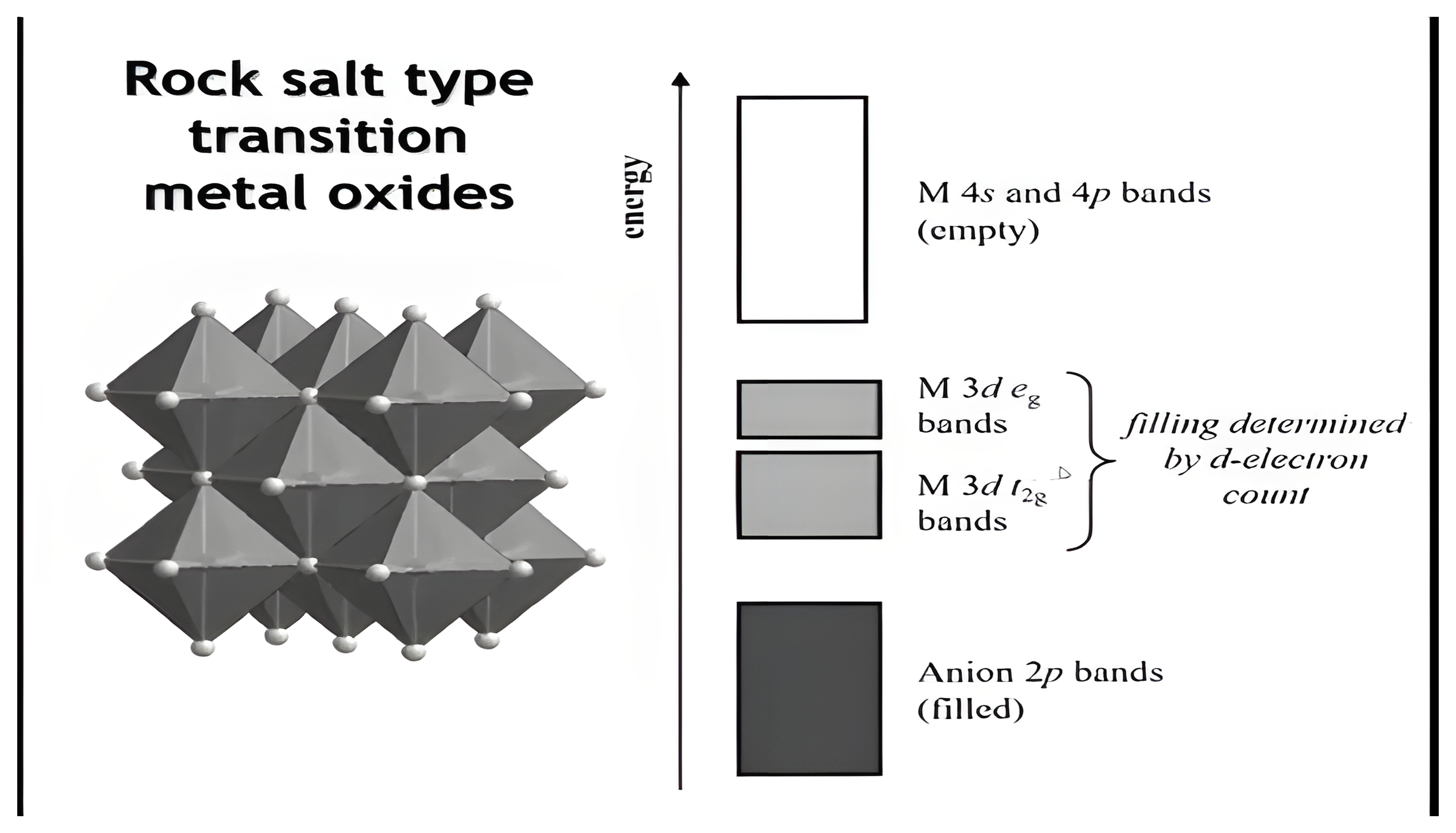
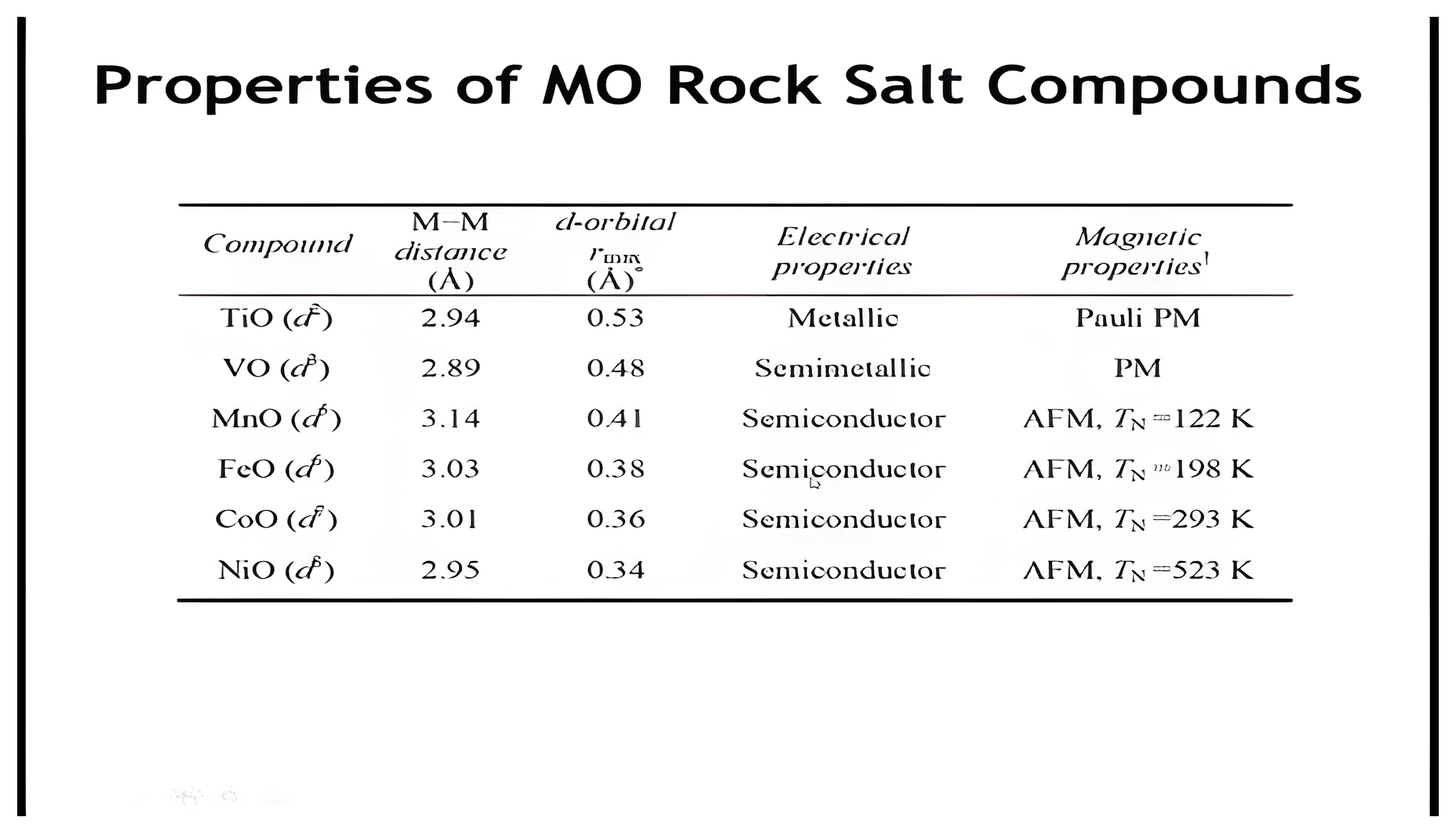
- Predict conductivity trends across rock salt structure oxides based on d-orbital contraction and metal-metal distance
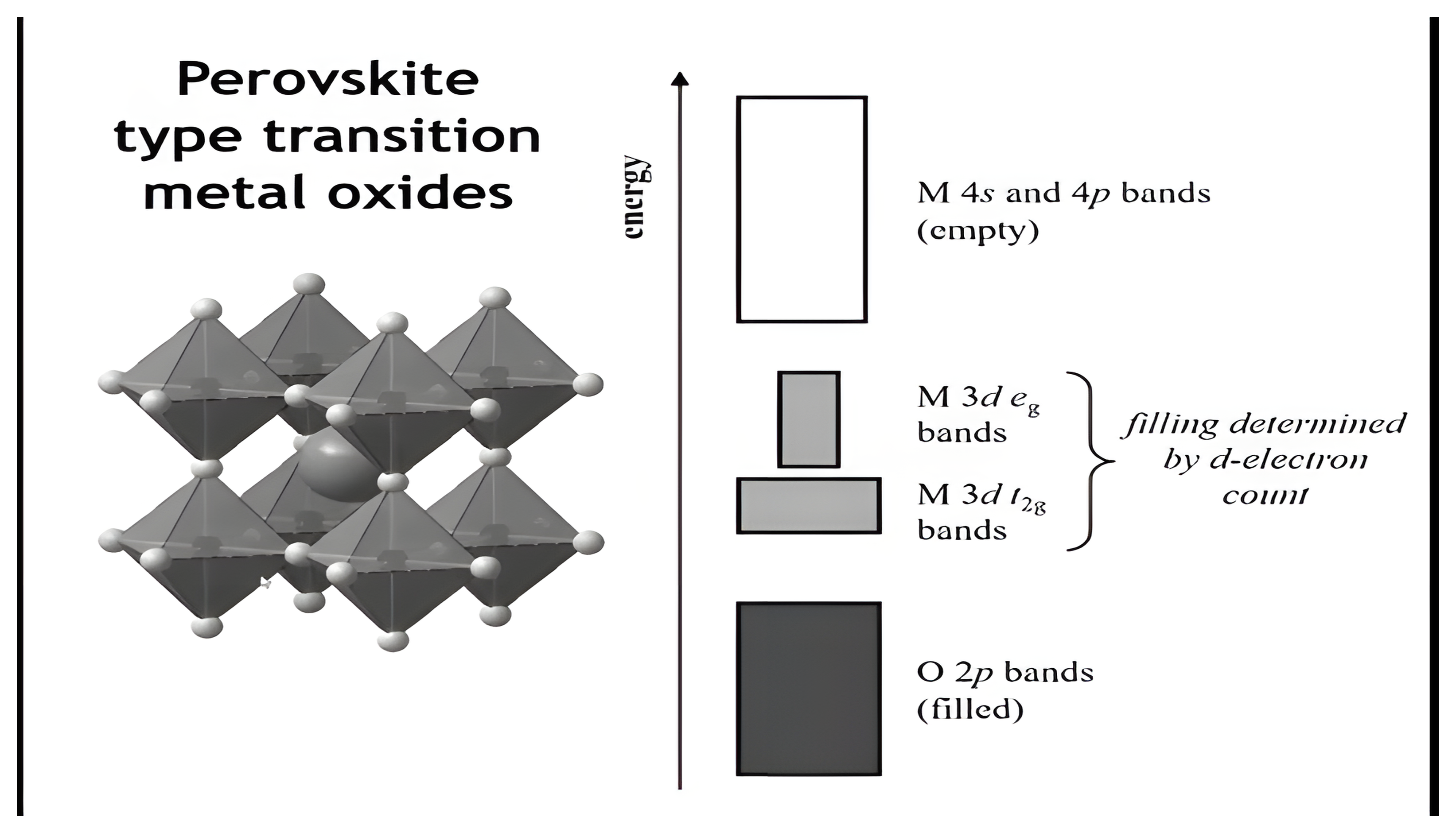
- Analyze conductivity patterns in perovskite structures and explain differences between 3+ and 4+ oxidation states
Conductivity of Select Materials: NiO and TiO
| Substance | σ (S/m) | Substance | σ (S/m) |
|---|---|---|---|
| Ag | 6.2 × 10⁷ | Bi₂Ru₂O₇ | 2 × 10⁵ |
| Cu | 5.9 × 10⁷ | LaNiO₃ | 1 × 10⁵ |
| Al | 3.8 × 10⁷ | doped polyacetylene | 8 × 10⁴ |
| Na | 2.1 × 10⁷ | Fe₃O₄ | 2 × 10⁴ |
| ReO₃ | 1.1 × 10⁷ | YBa₂Cu₃O₇ | 1 × 10² |
| Ti | 2.5 × 10⁶ | Ge | 2 × 10⁰ |
| La | 1.6 × 10⁶ | Si | 10⁻³ |
| SrMoO₃ | 1.0 × 10⁶ | NiO | 10⁻⁸ |
| Bi | 7.7 × 10⁵ | Al₂O₃ | 10⁻¹² |
| Mn | 6.2 × 10⁵ | S | 10⁻¹⁵ |
| NbN | 4 × 10⁵ | SiO₂ (Quartz) | 10⁻¹⁶ |
| TiO | 3 × 10⁵ | Teflon | 10⁻²² |
Conduction on a Ti³⁺ (d¹) Lattice
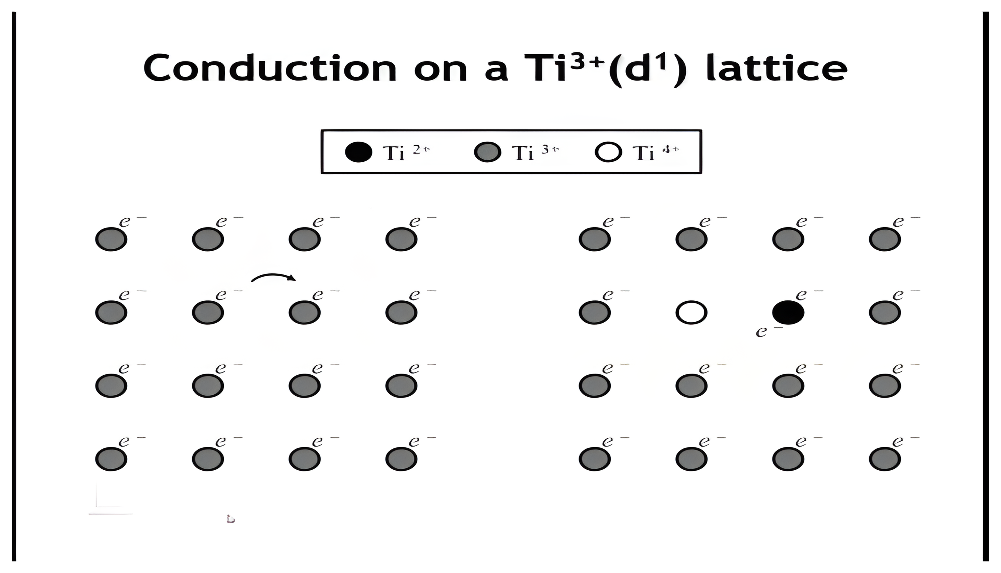
Hubbard U
The Hubbard model considers interactions (repulsions) between electrons on the same site, while neglecting longer range electron-electron interactions. The strength of the onsite electron-electron interactions is given by the Hubbard U, which we can estimate for gas phase ions.
| Ti³⁺(g) → Ti⁴⁺(g) + e⁻ | IE of Ti³⁺ = 4th IE of Ti = 43.3 eV |
| Ti³⁺(g) + e⁻ → Ti²⁺(g) | Heg of Ti³⁺ = −(3rd IE of Ti) = −29.3 eV |
| 2 Ti³⁺(g) → Ti⁴⁺(g) + Ti²⁺(g) | U = IE + Heg = 14.0 eV |
In a solid U is smaller (2-5 eV for 3d TM ions) because:
- the surrounding lattice is polarized by the charge of the site
- the electron wavefunctions are more spread out than they are on a gas phase ion
Heg (electron gain enthalpy) is equivalent to electron affinity (with the opposite sign)
The $d_{xy}$ Band in a Square TiN Plane
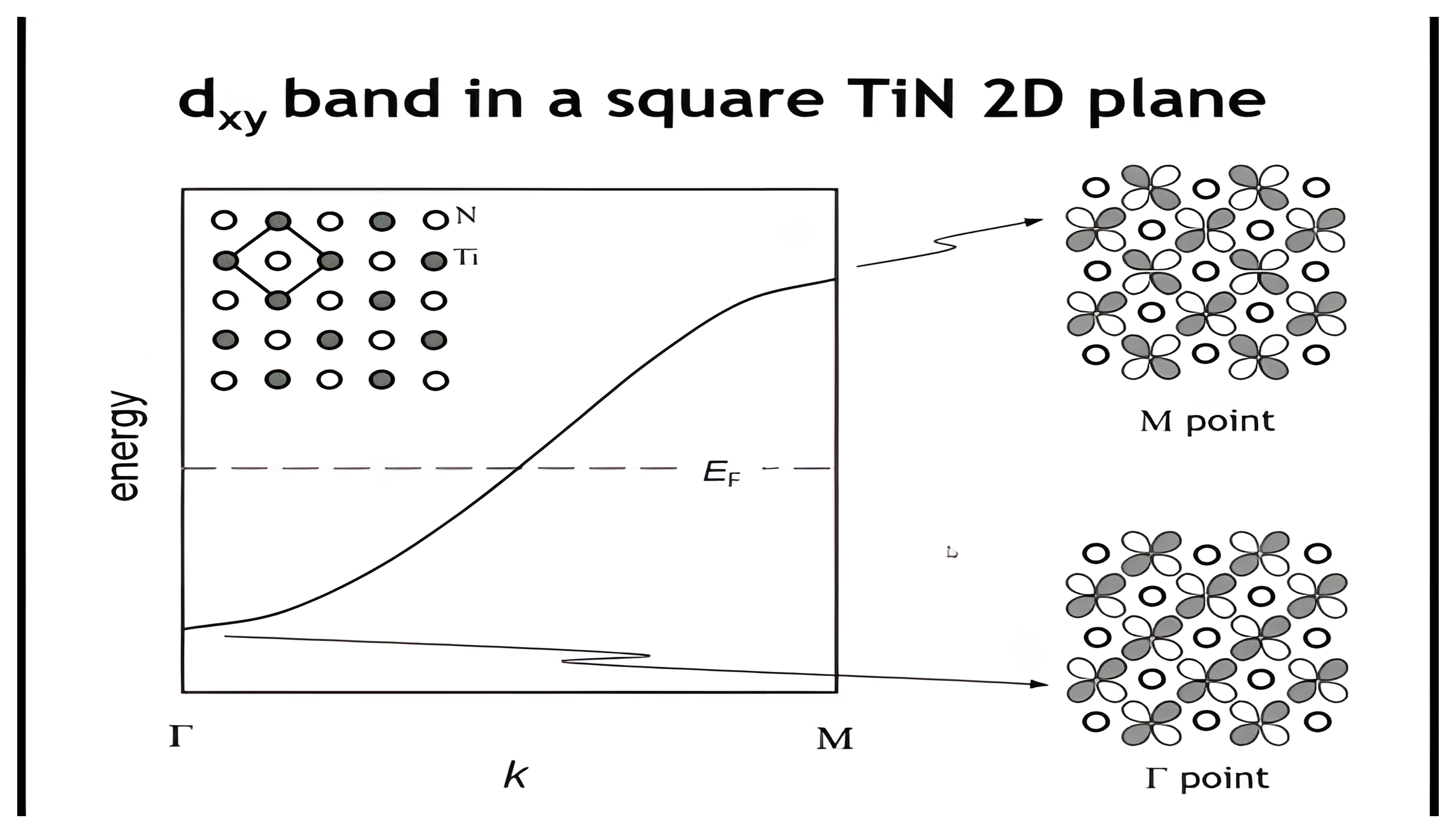
Mott-Hubbard Insulator
Rock Salt Transition Metal Oxides
Properties of MO Rock Salt Compounds
Perovskite Transition Metal Oxides
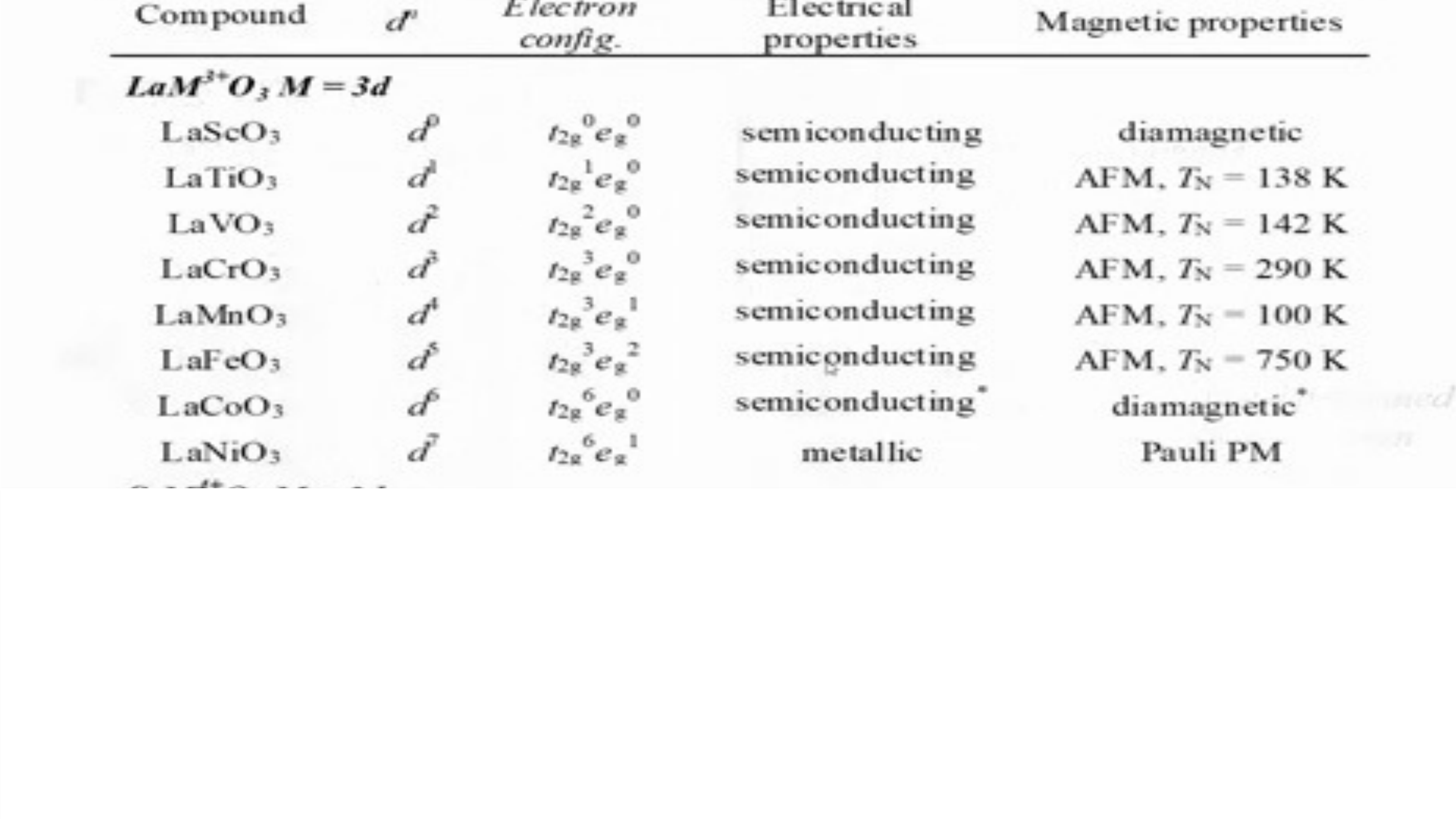
Perovskites with M³⁺ and M⁴⁺ Ions
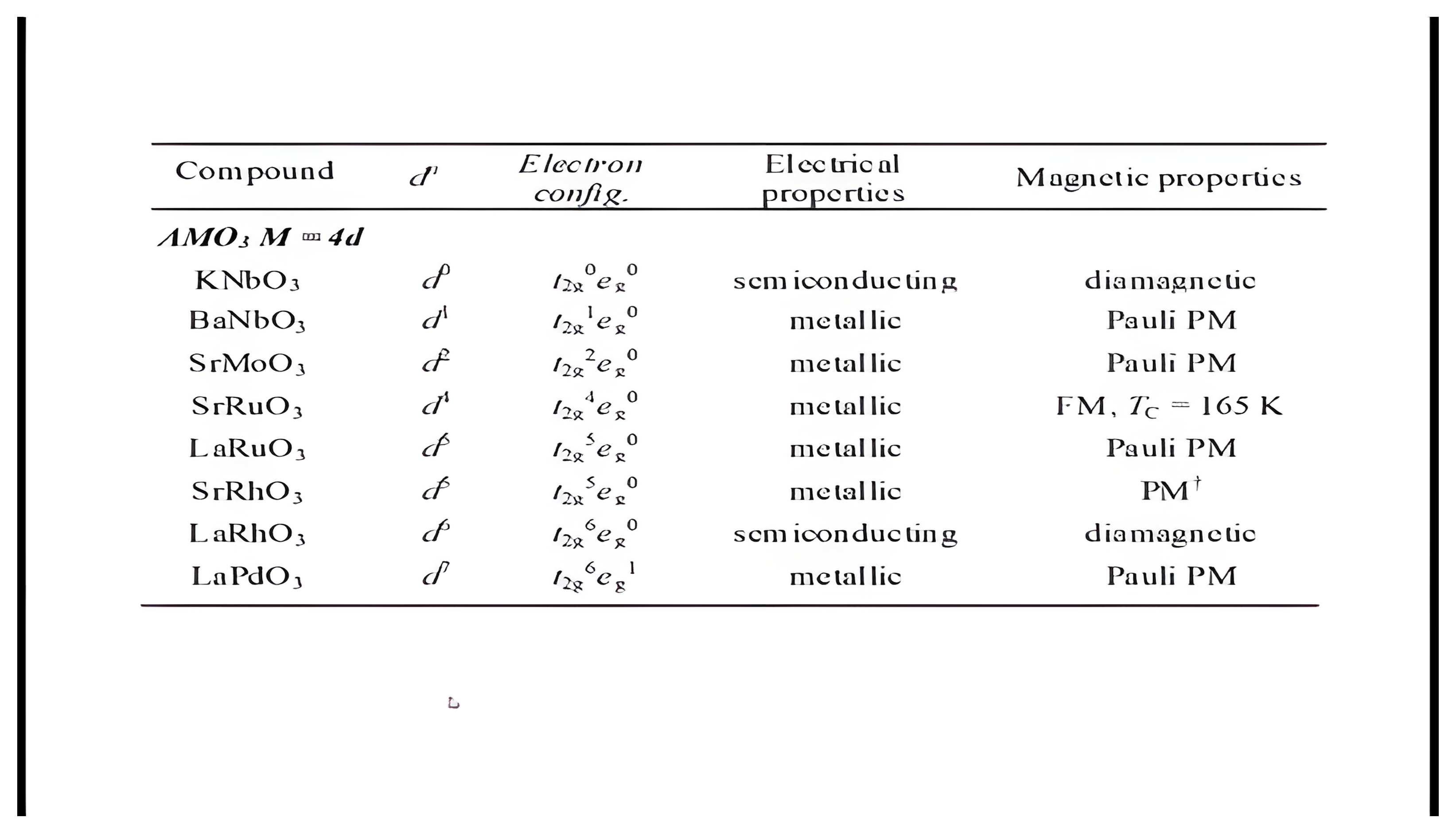
4d Perovskites
See Gradescope Quiz 3
1. Which of the following best explains the dramatic difference in conductivity between NiO and TiO, despite both having the rock salt structure and partially filled d-orbitals?
2. In the context of the Hubbard model, which condition is most likely to lead to a Mott-Hubbard insulator?
3. Considering transition metal oxides with the rock salt structure (TiO, VO, MnO), why does the conductivity trend from metallic (TiO) to semiconducting (MnO) as we move across the period?
4. Strontium manganate (SrMnO₃) is a semiconductor, even though other 4+ perovskites exhibit metallic behavior. This is attributed to a particularly large Hubbard U. What characteristic of the Mn⁴⁺ (d³) electron configuration contributes to this exceptionally large U?
Conductivity of Select Materials: Conducting Polymers
Practice questions
Work the Lecture 20 practice questions before the next class. They cover intrinsic and doped semiconductors, the p-n junction and its devices, the Hubbard model, and conductivity trends in transition metal oxides.
Open the Lecture 20 practice questions
Every question carries a worked explanation, so you can check your reasoning as you go.